
Capacitor type fingerprint sensor

A fingerprint sensor, capacitive technology, applied in the direction of acquiring/arranging fingerprints/palmprints, instruments, characters and pattern recognition, etc., can solve the problems of small effective signal, easy saturation of the integrator, and small output dynamic range of the integrator. To achieve the effect of increasing the dynamic range

Active Publication Date: 2017-02-22
SHENZHEN GOODIX TECH CO LTD
View PDF8 Cites 6 Cited by
  • Summary
  • Abstract
  • Description
  • Claims
  • Application Information

AI Technical Summary

Problems solved by technology

[0005] However, during fingerprint collection, due to the parasitic capacitance in the fingerprint sensor, or the substrate capacitance in the fingerprint capacitor, a large substrate signal will be generated at the output of the integrator, and the magnitude of the substrate signal is at least 100 times the effective signal , after being amplified by the amplifier, the base signal is much larger than the effective signal, causing the effective signal to appear smaller. At the same time, after the base signal is amplified, the integrator is easy to reach saturation, which leads to a smaller output dynamic range of the integrator.

Method used


Image

  • Capacitor type fingerprint sensor
  • Capacitor type fingerprint sensor
  • Capacitor type fingerprint sensor

Examples


Embodiment Construction

[0018] The implementation of the present application will be described in detail below in conjunction with the drawings and examples, so that the realization process of how the present application uses technical means to solve technical problems and achieve technical effects can be fully understood and implemented accordingly.

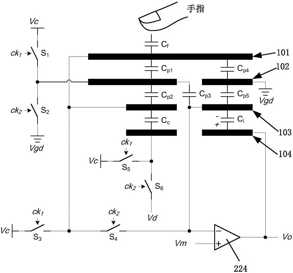
[0019] figure 1 It is a schematic diagram of a typical fingerprint sensor structure; figure 1 As shown, the fingerprint sensor produced according to one layer of polysilicon six-layer metal (referred to as 1P6M) may include N-th layer metal 101, N-1-th layer metal 102, N-2-th layer metal 103, N-3-th layer metal 104, Where N represents the uppermost layer of metal in the fingerprint sensor manufacturing process. In this embodiment, N is equal to 6, and the Nth layer of metal 101 is the sixth layer of metal, the N-1st layer of metal 102 is the fifth layer of metal, and the N-2nd layer of metal Layer metal 103 is the fourth layer of metal, N-3th layer of...


PUM


Abstract

The embodiment of the invention provides a capacitor type fingerprint sensor. The capacitor type fingerprint sensor includes a first pole plate layer, a second pole plate layer and a third pole plate layer which are successively arranged; the first pole plate layer and a finger form a finger capacitor; at least one fourth pole plate layer is arranged between the first pole plate layer and the second pole plate layer; a first parasitic capacitor is formed between the first pole plate layer and the fourth pole plate layer; a second parasitic capacitor is formed between the second pole plate layer and the fourth pole plate layer; the capacitor type fingerprint sensor includes an integrator having an integrating capacitor which formed between the second pole plate layer and the third pole plate layer; and the first parasitic capacitor and the second parasitic capacitor are invisible for the integrating capacitor, and the integrating capacitor is used for storing charges from the fingerprint capacitor.

Description

technical field [0001] Embodiments of the present invention relate to the technical field of biological feature identification, and in particular to a capacitive fingerprint sensor. Background technique [0002] Since the fingerprint has lifelong invariance, uniqueness and convenience, it can provide a higher level of identity security authentication. When performing identity security authentication, a fingerprint sensor (also known as Fingerprint Sensor) is usually used as a device for realizing automatic fingerprint collection. [0003] Fingerprint sensors are mainly divided into optical fingerprint sensors, semiconductor capacitive sensors, semiconductor thermal sensors, semiconductor pressure sensors, ultrasonic sensors and radio frequency (RF) sensors according to the sensing principle. [0004] Taking the semiconductor capacitive sensor as an example, on a "flat plate" integrated with tens of thousands of semiconductor devices, a finger is pasted on it to form the oth...

Claims


Application Information

Patent Timeline
IPC IPC(8): G06K9/00G06V30/144
CPCG06V40/1306G06F21/32
Inventor 张孟文詹昶皮涛林碧荣
Owner SHENZHEN GOODIX TECH CO LTD
Learn More