Serial feature tracking for endpoint detection

A sequence and end-point technology, applied in the direction of grinding machine parts, workpiece feed motion control, grinding machine tools, etc., can solve problems such as the inability to meet the growing demand of semiconductor device manufacturing, and achieve improved wafer-to-wafer thickness consistency, Improved end-point control

Active Publication Date: 2017-02-22
APPLIED MATERIALS INC
View PDF5 Cites 3 Cited by
  • Summary
  • Abstract
  • Description
  • Claims
  • Application Information

AI Technical Summary

Problems solved by technology

However, existing optical monitoring techniques may not be able to meet the increasing demands of semiconductor device manufacturing

Method used


Image

  • Serial feature tracking for endpoint detection
  • Serial feature tracking for endpoint detection
  • Serial feature tracking for endpoint detection

Examples


Embodiment Construction

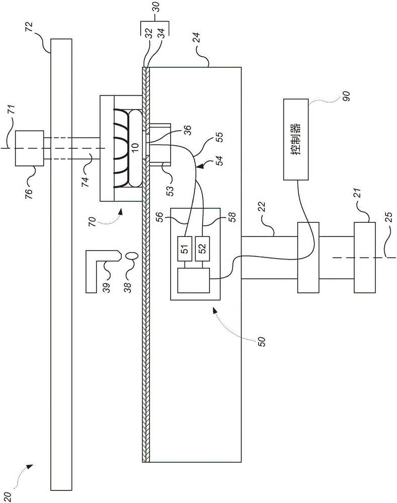
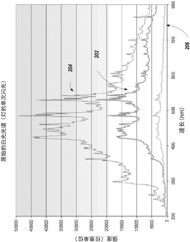
[0017] An optical monitoring technique is used to measure the spectrum of light reflected from a substrate being polished and to track the properties of spectral features (eg, track the position of peaks in the measured spectrum). The modification of the polishing process may be performed based on the value of the property across predetermined boundaries and / or may be changed by a predetermined amount by the property, (e.g., based on crossing a boundary calculated by adding the predetermined amount to the initial value of the property). Modify or trigger the polishing endpoint.

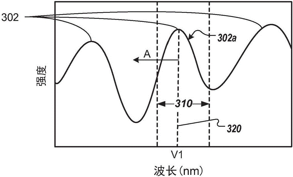
[0018] However, for some layer structures on the substrate, features may shift too much, for example, the wavelength position of a peak may shift completely across the wavelength band being monitored by the spectroscopic system before polishing is complete. A technique used to solve this problem is to serially "stitch" the tracks of multiple features together. For example, once the wavelength of the ...


PUM


Abstract

A method of controlling polishing includes polishing a substrate having a second layer overlying a first layer, detecting exposure of the first layer with an in-situ monitoring system, receiving an identification of a selected spectral feature and a characteristic of the selected spectral feature to monitor during polishing, measuring a sequence of spectra of light from the substrate while the substrate is being polished, determining a first value for the characteristic of the feature at the time that the first in-situ monitoring technique detects exposure of the first layer, adding an offset to the first value to generate a second value, and monitoring the characteristic of the feature and halting polishing when the characteristic of the feature is determined to reach the second value.

Description

technical field [0001] The present disclosure is related to optical monitoring during chemical mechanical polishing of a substrate. Background technique [0002] Integrated circuits are typically formed on a substrate by sequentially depositing conductive, semiconductive, or insulating layers on a silicon wafer. One fabrication step involves: depositing a filler layer on a non-planar surface; and planarizing the filler layer. For some applications, the filler layer is planarized until the top surface of the patterned layer is exposed. For example, a conductive filler layer may be deposited on the patterned insulating layer to fill trenches or holes in the insulating layer. After planarization, the conductive partial layers remaining between the raised patterns of the insulating layer form vias, plugs and lines that provide conductive paths between the thin film circuits on the substrate. For other applications (such as oxidation polishing), the filler layer is planarized ...

Claims


Application Information

Patent Timeline
Patent Type & Authority Applications(China)
IPC IPC(8): H01L21/304
CPCB24B49/12B24B37/013H01L21/304
Inventor J·D·大卫
Owner APPLIED MATERIALS INC
Why Eureka
Try Eureka