Semiconductor silicon-based optical waveguide device and preparation method thereof

A silicon-based optical waveguide and semiconductor technology, used in optical waveguides, optical components, light guides, etc., can solve the problem of high dependence on substrate quality, achieve flexible design and manufacturing, broad application prospects, yield and integration. high effect

Active Publication Date: 2019-04-23
JILIN SINO MICROELECTRONICS CO LTD
View PDF4 Cites 2 Cited by
  • Summary
  • Abstract
  • Description
  • Claims
  • Application Information

AI Technical Summary

Problems solved by technology

[0004] The first object of the present invention is to provide a method for preparing semiconductor silicon-based optical waveguide devices, which solves the problem that conventional waveguide devices use quartz substrates, which are highly dependent on the quality of substrates and require special quartz processing equipment to be manufactured. technical problem

Method used


Image

  • Semiconductor silicon-based optical waveguide device and preparation method thereof

Examples


preparation example Construction

[0035] According to a first aspect of the present invention, the present invention provides a method for preparing a semiconductor silicon-based optical waveguide device, comprising the following steps:

[0036] (a) Deposit the bottom cladding layer on the non-polished surface of the single-sided polished silicon wafer;

[0037] (b) sequentially stacking and depositing the lower cladding layer, core layer and mask layer on the polished surface of the single-sided polished silicon wafer;

[0038] (c) forming a waveguide channel after etching the core layer and removing the mask layer;

[0039] (d) Depositing an upper cladding layer on the etched core layer to obtain a semiconductor silicon-based optical waveguide device;

[0040] Preferably, the mask layer is a metal mask layer.

[0041] The preparation method of the semiconductor silicon-based optical waveguide device provided by the present invention uses semiconductor silicon as the substrate material, has good compatibili...

Embodiment 1

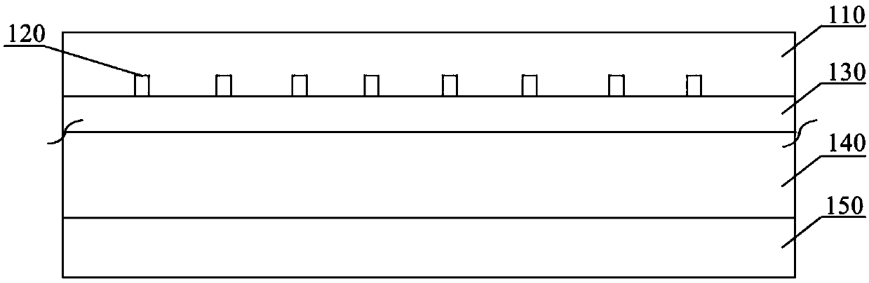
[0104] This embodiment provides a semiconductor silicon-based optical waveguide device, the structure of which is as follows figure 1 As shown, there are bottom cladding layer 150 , single-sided polished silicon wafer 140 , lower cladding layer 130 , waveguide channel 120 and upper cladding layer 110 from bottom to top. Its preparation method comprises the following steps:

[0105] (a) Select a general-purpose single-sided polished silicon wafer 140 for cleaning before deposition, and then use PECVD equipment to deposit a bottom cladding layer 150 on the non-polished surface of the single-sided polished silicon wafer 140. The bottom cladding layer 150 is boron-phosphorus-doped Silicon dioxide, wherein the mass ratio of borane to silicon dioxide is 1.7:100, the mass ratio of phosphine to silicon dioxide is 1.9:100, and the thickness is 18 μm.

[0106] (b) Use megasonic dilute hydrofluoric acid solution and SC-1 solution to clean the single-sided polished silicon wafer 140, and...

Embodiment 2

[0111] This embodiment provides a semiconductor silicon-based optical waveguide device. The difference between the preparation method of this embodiment and Embodiment 1 is that the thickness of the core layer is 5.5 μm, and 8 channels (5.5 μm ×5.5μm cross-sectional area) splitter optical waveguide device.


PUM


Abstract

The invention provides a semiconductor silicon-based optical waveguide device and a preparation method thereof, and relates to the field of optical waveguide chip producing and manufacturing. The preparation method of the semiconductor silicon-based optical waveguide device comprises the following steps that (a) a bottom cladding layer is deposited on a non-polished surface of a single-surface-polished silicon wafer; (b) a lower cladding layer, a core layer and a mask layer are deposited in an overlapped mode in sequence on a polished surface of the single-surface-polished silicon wafer; (c) awaveguide channel is formed after the core layer is etched, and the mask layer is removed; and (d) an upper cladding layer is deposited on the etched core layer, and thus the semiconductor silicon-based optical waveguide device is obtained. Preferably, the mask layer is a metal mask layer, and the technical problems that quartz substrate slices are used in conventional waveguide devices, the dependency on the quality of the substrate slices is high and special quartz processing equipment needs to be ordered for manufacturing are solved. According to the preparation method of the semiconductorsilicon-based optical waveguide device, semiconductor silicon is adopted as a substrate slice, compatibility with silicon semiconductor manufacturing equipment is good, the influence of the substrateslice refractive index is avoided, and design and manufacturing are more flexible.

Description

technical field [0001] The invention relates to the field of optical waveguide chip production and manufacturing, in particular to a semiconductor silicon-based optical waveguide device and a preparation method thereof. Background technique [0002] At present, planar optical waveguide splitters are very popular in domestic and foreign markets. According to the report of market and technology consulting company ElectroniCast on April 5, 2016, the global planar optical waveguide splitter market totaled 696 million US dollars in 2015, a year-on-year increase of 14%. . China has now become the dominant player in the planar optical waveguide splitter market, accounting for more than 35% of the total market. Before 2012, domestic optical splitter devices were all imported from South Korea and Japan, and only packaging was available in China, and most of the profits were taken by South Korea, Japan, Europe and the United States. After years of painstaking research and developmen...

Claims


Application Information

Patent Timeline
Patent Type & Authority Applications(China)
IPC IPC(8): G02B6/12
CPCG02B6/12G02B2006/12061G02B2006/1215G02B2006/12166
Inventor 孙喆禹邢文超孙宣夏忠财杨寿国
Owner JILIN SINO MICROELECTRONICS CO LTD
Why Eureka
Try Eureka