Asymmetric half-bridge flyback converter and driving control method therefor
A flyback converter, drive control technology, applied in control/regulation systems, DC power input conversion to DC power output, instruments, etc., can solve problems such as large loss of asymmetrical half-bridge flyback converters
- Summary
- Abstract
- Description
- Claims
- Application Information
AI Technical Summary
Problems solved by technology
Method used
Image
Examples
no. 1 example
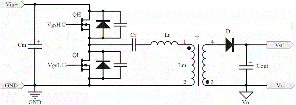
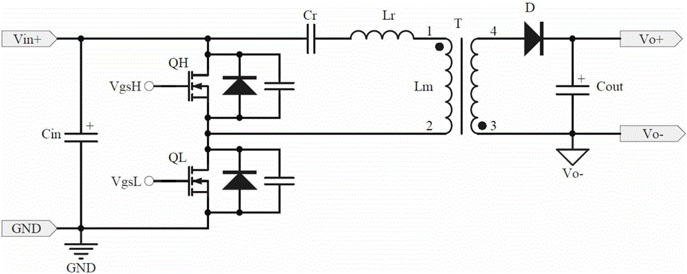
[0050] Figure 3-1 Shows the circuit principle block diagram of the asymmetrical half-bridge flyback converter of the first embodiment of the present invention, Figure 3-2 It is the schematic circuit diagram of the first embodiment of the present invention. The asymmetrical half-bridge flyback converter includes a flyback circuit and a detection control circuit; the flyback circuit includes a primary side circuit and a secondary side output rectification and filtering circuit. The primary side circuit is composed of filter capacitor Cin, resonant capacitor Cr, main switch tube QH, clamp switch tube QL and the primary winding of the transformer T, Lr is the leakage inductance of the primary winding of the transformer T; one end of Cin is connected to the input The positive pole Vin+, the other end is connected to the input ground GND (or the input negative pole), the drain of the main switching tube QH is connected to Vin+, the source is connected to the drain of the clamping...
no. 2 example
[0078] Such as Figure 5 As shown, it is a schematic circuit diagram of the second embodiment of the asymmetrical half-bridge flyback converter according to the present invention, and the dotted box 502 is the drive control module.
[0079]Compared with the first embodiment of the present invention, the difference of the second embodiment is that a driver IC2 is added between the drain output terminal of the N-MOS transistor and the gate of the clamp switch QL for Drive the clamping switch QL more quickly, the input terminal of the driving IC2 is connected to the drain of the N-MOS transistor Q1, the output terminal of the driving IC2 is connected to the gate of QL, and the voltage at the output terminal of the driving IC2 follows the change of the voltage at the input terminal; After IC2 is driven, the driving capability of the entire detection control circuit is enhanced. The working principle of the second embodiment of the present invention is basically the same as that of...
no. 3 example
[0097] Such as Figure 6-1 As shown, it is the schematic circuit diagram of the third embodiment of the asymmetrical half-bridge flyback converter according to the present invention, and the dotted box 601 is the detection control circuit.
[0098] The difference from the first embodiment is the drive control module part. In the third embodiment, the VOB pin of the drive IC1 outputs the drive voltage signal VgsL, and VgsL is connected to the first pin of the first current limiting resistor R11, and the first current limiting The second pin of the resistor R11 is connected to the base of the charging transistor TR1, and also connected to the cathode of the Zener diode Z1, and the anode of the Zener diode Z1 is connected to the input ground GND (that is, the input negative pole of the asymmetrical half-bridge flyback converter); The driving voltage signal VgsL is also connected to the first pin of the second current limiting resistor R12, and the second pin of the second current...
PUM
 Abstract
Description
Claims
Application Information


