Chip packaging structure and preparation method thereof

A chip packaging structure and chip technology, applied in semiconductor/solid-state device manufacturing, electrical components, electric solid-state devices, etc., can solve problems such as high cost, chip damage, and easy warpage, and achieve warpage control and low material cost , the effect of expanding the utilization rate

Inactive Publication Date: 2017-03-22
NAT CENT FOR ADVANCED PACKAGING
View PDF4 Cites 8 Cited by
  • Summary
  • Abstract
  • Description
  • Claims
  • Application Information

AI Technical Summary

Problems solved by technology

[0005] In view of this, an embodiment of the present invention provides a chip packaging structure and a manufacturing method thereof, so as to solve the technical problems of high cost, chip damage, and warpage in the manufacturing process of the existing fan-out chip

Method used


Image

  • Chip packaging structure and preparation method thereof
  • Chip packaging structure and preparation method thereof
  • Chip packaging structure and preparation method thereof

Examples


Embodiment

[0042] Embodiments of the present invention provide a chip packaging structure and a manufacturing method thereof. figure 1 It is a schematic flow chart of a method for preparing a chip packaging structure provided by an embodiment of the present invention, such as figure 1 As shown, the method for preparing the chip package structure provided by the embodiment of the present invention may include the following steps:

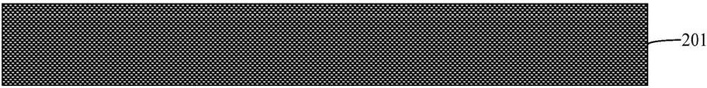
[0043] S110. Provide a carrier plate, prepare a double-layer peeling structure on the upper and lower surfaces of the carrier plate, and the double-layer peeling structure includes an upper layer structure and a lower layer structure.

[0044] Exemplary, figure 2 is a schematic cross-sectional view of the carrier plate provided by the embodiment of the present invention, such as figure 2 As shown, the material of the carrier 201 can be silicon, silicon dioxide, ceramics, glass, metal, alloy, and organic material, etc., and the shape of the carrier can be re...


PUM


Abstract

The invention discloses a chip packaging structure and a preparation method thereof. The preparation method comprises the following steps: providing a support plate, and preparing double-layer peeling structures on the upper surface and the lower surface of the support plate; preparing a rewiring layer on the side, away from the support plate, of each double-layer peeling structure; preparing first dielectric layers on each rewiring layer and the surface of each double-layer peeling structure; preparing at least one blind hole in each first dielectric layer; filling a conducting material in the blind holes; providing a chip, and arranging the chip on each first dielectric layer; preparing a second dielectric layer on the periphery of each chip, wherein each first dielectric layer is covered with the corresponding second dielectric layer, and each chip is wrapped by the corresponding second dielectric layer; peeling off the double-layer peeling structures; etching an upper-layer structure of each double-layer peeling structure so as to expose the corresponding rewiring layer and the corresponding first dielectric layer; and preparing a welded ball on the side, away from each first dielectric layer, of the corresponding rewiring layer, wherein each welded ball is electrically connected with the corresponding rewiring layer. To sum up, the preparation method is simple, high in operability and low in cost, and can avoid chip damage; and moreover, preparation technology is carried out on two sides of the support plate simultaneously, so that the efficiency is high, and warping is avoided.

Description

technical field [0001] The embodiments of the present invention relate to the technical field of chip packaging, and in particular to a chip packaging structure and a manufacturing method thereof. Background technique [0002] With the continuous development of information technology and semiconductor technology, electronic devices such as mobile phones, PADs, and smart watches are gradually showing a trend of light weight and integrated functions. This has higher and higher requirements for the integration of chips in electronic equipment, which in turn brings unprecedented challenges to chip packaging. Increasing interconnect pitch mismatches, adding various chips with different functions, and reducing package size in the same footprint to increase battery size for longer life have opened windows for innovative embedded packaging technologies. [0003] Benefiting from the development of 3D Through Silicon Vias (TSV) technology, Fan-Out Wafer Level Packaging (FOWLP) is cur...

Claims


Application Information

Patent Timeline
Patent Type & Authority Applications(China)
IPC IPC(8): H01L21/56H01L23/31H01L23/498
CPCH01L2224/16235H01L2224/18H01L2224/81005H01L2924/15311H01L2924/15313H01L2924/3511H01L23/31H01L21/56H01L23/498
Inventor 郭学平郝虎于中尧
Owner NAT CENT FOR ADVANCED PACKAGING
Why Eureka
Try Eureka