Preparation method and use method for test sample used for measuring length of lightly doped drain

A lightly doped drain region and test sample technology, applied in semiconductor/solid-state device testing/measurement, semiconductor/solid-state device manufacturing, electrical components, etc., can solve product characterization and measurement, LDD deviation, and inability to effectively monitor LDD Doping process and other issues to achieve the effect of improving stability and reliability

Active Publication Date: 2017-05-10
WUHAN CHINA STAR OPTOELECTRONICS TECH CO LTD
View PDF3 Cites 0 Cited by
  • Summary
  • Abstract
  • Description
  • Claims
  • Application Information

AI Technical Summary

Problems solved by technology

[0006] However, when producing LTPS array substrates, the existing production lines can only estimate the length of the LDD based on the length of the photoresist, but cannot perform the characterization and measurement of the actual product
like Figure 1a , Figure 1b ,and Figure 1c As shown, LDD is formed by doping polysilicon (poly-Si) with ions. After ion implantation into polysilicon, a small amount of diffusion will be carried out through the subsequent activation process. The actual length of LDD will have a certain deviation from the estimated value. Therefore, the existing method of estimating the length of the lightly doped drain region of the TFT in the LTPS array substrate cannot effectively monitor the LDD doping process.

Method used


Image

  • Preparation method and use method for test sample used for measuring length of lightly doped drain
  • Preparation method and use method for test sample used for measuring length of lightly doped drain
  • Preparation method and use method for test sample used for measuring length of lightly doped drain

Examples


Embodiment Construction

[0050] In order to further illustrate the technical means adopted by the present invention and its effects, the following describes in detail in conjunction with preferred embodiments of the present invention and accompanying drawings.

[0051] see figure 2 , the present invention firstly provides a method for making a test sample for measuring the length of a lightly doped drain region, comprising the following steps:

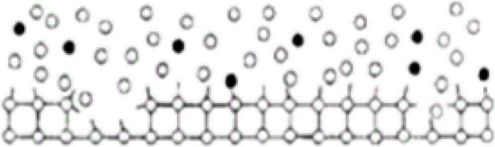
[0052] Step S1, such as image 3 As shown, a base substrate 1 is provided, and a covering buffer layer 2 is deposited on the base substrate 1 .

[0053]The base substrate 1 is preferably a glass substrate; the material of the buffer layer 2 is silicon nitride (SiNx), silicon oxide (SiOx), or a combination of both.

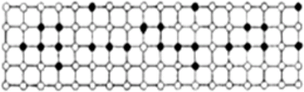
[0054] Step S2, such as Figure 4 As shown, an amorphous silicon layer is deposited on the buffer layer 2, and the amorphous silicon layer is crystallized to obtain a polysilicon layer 3', and the polysilicon layer 3' is patterned.

[0055] In...


PUM


Abstract

The invention provides a preparation method and a use method for a test sample used for measuring the length of a lightly doped drain. According to the preparation method, light resistance (7) on an interlayer insulation layer (6) is subjected to exposure and development to ensure that the light resistance (7) above a lightly doped drain (33) and the periphery of the lightly doped drain is removed by development, then the residual light resistance (7) is taken as a shielder, the interlayer insulation layer (6) and a gate insulation layer (4) are subjected to dry etching, and a gate (5), the lightly doped drain (33) and at least part of a heavily doped region (32) connected with the lightly doped drain (33) are exposed; and a vertical view image of the test sample is shot by using an electron scanning microscope in a production line, and the length, namely, the actual length of the lightly doped drain (33), from the edge of the gate (5) to a boundary line of the lightly doped drain (33) and the heavily doped region (32) is measured on the vertical view image, so that a doping process of the LDD (Lightly Doped Drain) can be effectively monitored in the production line, and the product stability and reliability are improved.

Description

technical field [0001] The invention relates to the field of display device detection, in particular to a method for making and using a test sample for measuring the length of a lightly doped drain region. Background technique [0002] Thin Film Transistor (TFT) is the main driving element in current Liquid Crystal Display (LCD) and Active Matrix Organic Light-Emitting Diode (AMOLED). It is related to the display performance of the flat panel display device. [0003] Thin film transistors have various structures, and there are also various materials for preparing thin film transistors with corresponding structures. Low Temperature Polysilicon (LTPS) material is one of the more preferred materials. Due to the regular arrangement of atoms of low temperature polysilicon, the current carrying High sub-mobility. For voltage-driven LCDs, LTPS TFTs can use smaller TFTs to achieve deflection driving of liquid crystal molecules due to their high mobility, which greatly reduces the T...

Claims


Application Information

Patent Timeline
Patent Type & Authority Applications(China)
IPC IPC(8): H01L21/336H01L21/66
CPCH01L22/12H01L29/66492H01L29/66757
Inventor 孟林
Owner WUHAN CHINA STAR OPTOELECTRONICS TECH CO LTD
Why Eureka
Try Eureka