Manufacturing method of black film, black film and light-emitting device

A production method and black film technology, which are applied in the manufacture of electrical solid-state devices, semiconductor devices, and semiconductor/solid-state devices, etc., can solve the problems of difficulty in forming black films with surface morphology, and achieve the effect of smooth surface and good surface morphology.

Active Publication Date: 2017-05-10
NANJING TECH CORP LTD
View PDF9 Cites 2 Cited by
  • Summary
  • Abstract
  • Description
  • Claims
  • Application Information

AI Technical Summary

Problems solved by technology

[0006] The main purpose of this application is to provide a method for making a black film, a black film and a light-emitting device, so as to solve the problem that it is difficult to form a thicker black film with better surface morphology in the prior art

Method used


Image

  • Manufacturing method of black film, black film and light-emitting device
  • Manufacturing method of black film, black film and light-emitting device
  • Manufacturing method of black film, black film and light-emitting device

Examples


Embodiment 1

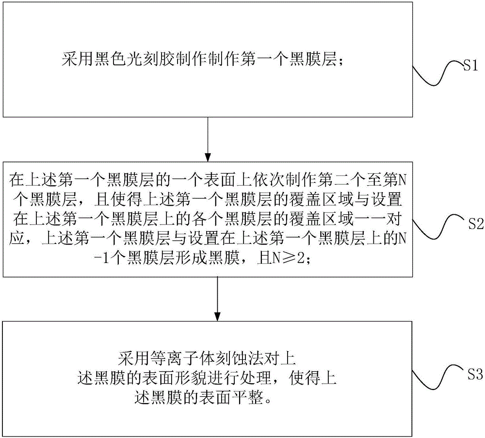
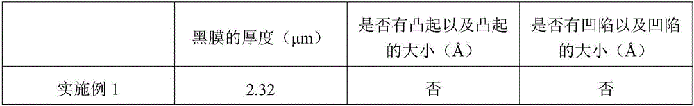
[0061] Pre-form a black film with a thickness of 2.3 μm, the specific production process is:

[0062] First, make the first black film layer.

[0063] A black photoresist is arranged on the surface of the substrate, and the thickness of the black photoresist is 1.3 μm; the black photoresist is pre-cured so that the black photoresist forms the first pre-black film layer that does not flow; the mask The plate is placed on the surface of the first pre-black film layer away from the substrate, and the light-transmitting area of ​​the mask plate includes the alignment mark, the light-transmitting area of ​​the mask plate and the coverage area of ​​the first pre-black film layer One-to-one correspondence; use ultraviolet light to expose the first pre-black film layer from the side of the mask away from the first pre-black film layer; developing to dissolve the unexposed areas in the first pre-black film layer; curing the developed first pre-black film layer to form the first black ...

Embodiment 2

[0071] The difference from Example 1 is that in the first gas, Ar and O 2 The molar ratio of the gas is 30:1, the ionization power of the first gas is 700W, and the etching time is 8s. In the second gas, He and N 2 65% of the total volume of the second gas, HF 1% of the total volume of the second gas, and O 2 The molar ratio with Ar is 6:1. And the ionization power of the second gas is 200W, and the etching time is 65s.

Embodiment 3

[0073] The difference from Example 1 is that in the first gas, Ar and O 2 The molar ratio of the first gas is 18:1, the ionization power of the first gas is 350W, and the etching time is 13s. The second gas does not include impurity removal gas, He and N 2 88% of the total volume of the second gas, and O 2 The molar ratio with Ar is 3:1. And the ionization power of the second gas is 500W, and the etching time is 28s.


PUM


Abstract

The invention provides a manufacturing method of a black film, the black film and a light-emitting device. The manufacturing method comprises the following steps of (S1) manufacturing a first black film layer by using a black photoresist; (S2) sequentially manufacturing a second black film layer to an Nth black film layer on one surface of the first black film layer, making a coverage area of the first black film layer correspond to the coverage areas of various black film layers arranged on the first black film layer one by one and forming a black film by the first black film layer and N-1 black film layers arranged on the first black film layer, wherein N is greater than or equal to 2; and (S3) processing the surface appearance of the black film by adopting a plasma etching method and making the surface of the black film smooth. According to the manufacturing method, the relatively thick black film can be manufactured, and the black film is relatively good in surface appearance and relatively smooth in surface.

Description

technical field [0001] The present application relates to the field of semiconductors, in particular, to a method for manufacturing a black film, a black film and a light emitting device. Background technique [0002] Black Mask (BM for short) is often set on the surface of the color filter (colorfilter) used in the liquid crystal panel. The black mask includes a plurality of grid areas or stripe areas for shading to cover adjacent pixels of different colors The boundary area between them, and then separate the red pixel, the green pixel and the blue pixel (ie RGB pixel). [0003] In the prior art, the preparation method of the black film usually needs to be completed with the help of ultraviolet light and a mask. The mask is set above the surface of the black photoresist, and the ultraviolet light source is set on a side of the mask away from the black photoresist. On the side, ultraviolet light passes through the mask to expose some areas of the black photoresist. The bla...

Claims


Application Information

Patent Timeline
Patent Type & Authority Applications(China)
IPC IPC(8): H01L51/56H01L51/52
CPCH10K50/865H10K71/00
Inventor 田庆海
Owner NANJING TECH CORP LTD
Why Eureka
Try Eureka