Switching power source control circuit and switching power source
A technology for controlling circuits and switching power supplies, which is applied in the direction of control/regulation systems, electrical components, and adjustment of electrical variables. It can solve the problems of shortened service life, increased loss, and high heat generation of power devices, so as to reduce losses, save costs, and improve efficiency effect
- Summary
- Abstract
- Description
- Claims
- Application Information
AI Technical Summary
Problems solved by technology
Method used
Image

Examples
Embodiment Construction
[0032] In order to have a clearer understanding of the technical features, purposes and effects of the present invention, the present invention will be further described in detail with reference to the accompanying drawings and embodiments.
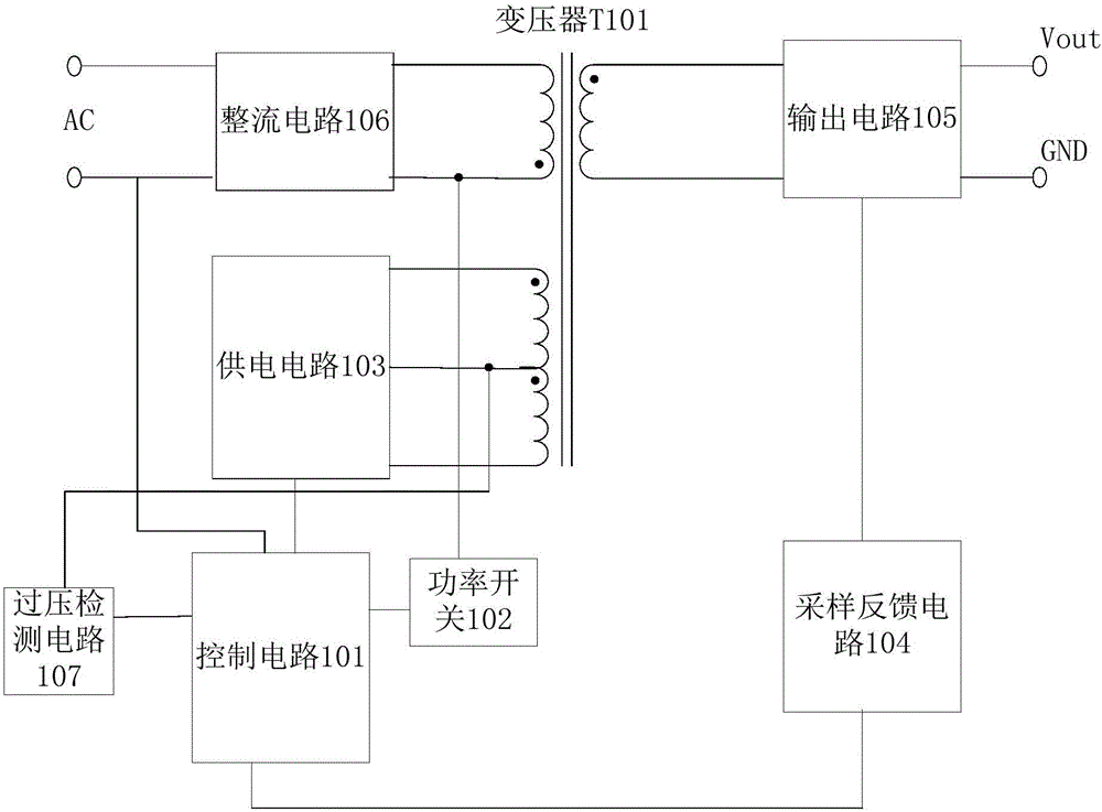
[0033] Aiming at the problems existing in the prior art, the present invention proposes a switching power supply control circuit. The switching power supply control circuit samples the voltage output by the switching power supply and feeds it back to the control circuit to adjust the current of the primary winding of the transformer, thereby regulating the voltage of the transformer. The output voltage of the auxiliary winding is to provide a suitable working voltage for the control circuit, so that the control circuit can work within the normal working range, reduce loss and prolong the service life of the switching power supply.
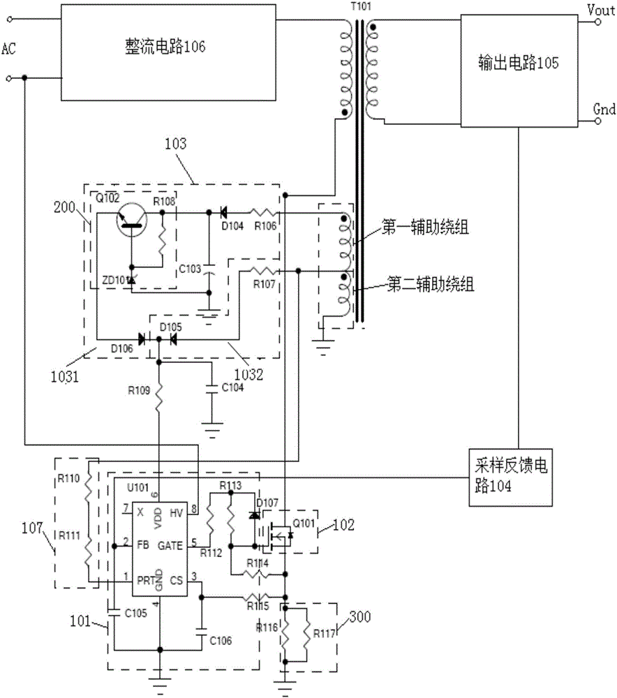
[0034] Such as figure 1 As shown, in the switching power supply control circuit of the present invention, t...
PUM
 Abstract
Description
Claims
Application Information
PatSnap Eureka turns technology decisions into work you can execute. Powered by our Innovation Knowledge Graph, it runs expert workflows across engineering, life sciences, materials and intellectual property. Get your review-ready output in minutes.


