Supercharge Your Innovation With Domain-Expert AI Agents!

CMOS differential modulation pulse detection circuit and method

A differential modulation and pulse detection technology, applied in the field of CMOS differential modulation pulse detection and integrated circuits, can solve the problems of low speed, large distortion of the modulated pulse detection circuit, and low precision, so as to improve the detection accuracy, eliminate common mode interference, improve the Effects of Signal Swing and Detection Accuracy

Inactive Publication Date: 2017-05-10
BEIJING INST OF RADIO MEASUREMENT
View PDF8 Cites 5 Cited by
  • Summary
  • Abstract
  • Description
  • Claims
  • Application Information

AI Technical Summary

Problems solved by technology

[0004] The technical problem to be solved by the present invention is to provide a CMOS differential modulation pulse detection circuit, the purpose of which is to solve the problems of large distortion, low speed and low precision of the modulation pulse detection circuit in the existing CMOS technology

Method used


Image

  • CMOS differential modulation pulse detection circuit and method
  • CMOS differential modulation pulse detection circuit and method
  • CMOS differential modulation pulse detection circuit and method

Examples


Embodiment 1

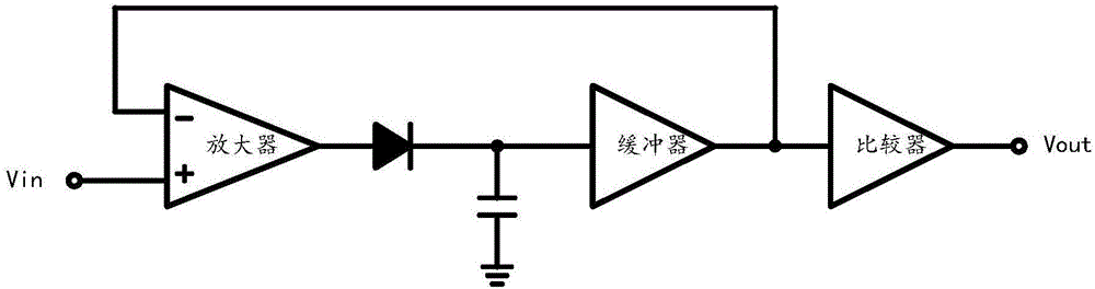
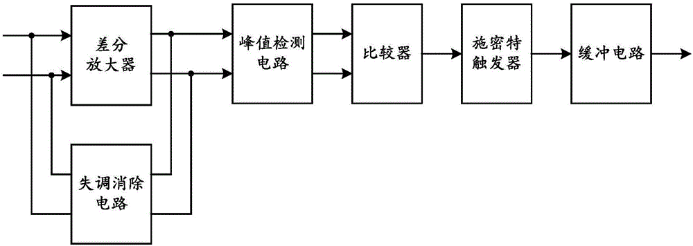
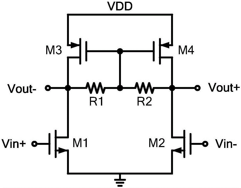
[0031] Such as figure 2 As shown, this embodiment proposes a CMOS differential modulation pulse detection circuit, the detection circuit includes a differential amplifier, an offset elimination circuit, a peak detection circuit, a comparator, a Schmitt trigger and a buffer circuit, the differential amplifier of the differential The signal input terminal receives the differential modulation pulse signal, the differential signal output terminal of the differential amplifier is connected to the differential signal input terminal of the offset elimination circuit and the differential signal input terminal of the peak detection circuit, and the peak detection signal output terminal of the peak detection circuit is connected to the peak value of the comparator The detection signal input terminal is connected, the comparison signal output terminal of the comparator is connected with the comparison signal input terminal of the Schmitt trigger, the trigger signal output terminal of the...

Embodiment 2

[0039] Such as Figure 9 As shown, this embodiment proposes a CMOS differential modulation pulse detection method, the method comprising:

[0040] S1, amplifying the input differential modulation pulse signal;

[0041] S2. Eliminate the offset voltage generated after amplifying the input differential modulation pulse signal;

[0042] S3. Detecting the high peak value and low peak value of the differentially modulated pulse signal;

[0043] S4. Perform edge shaping on the signal after peak detection;

[0044] S5. Eliminate the burrs of the signal output after the edge shaping;

[0045] S6. Providing a driving force for the output of the pulse signal.

[0046] The present invention adopts a differential amplifier and an offset elimination circuit structure to effectively eliminate common-mode interference, eliminate the influence of amplifier offset on detection, and improve detection accuracy; the peak detection circuit detects high and low peaks respectively, thereby impro...


PUM


Abstract

The invention relates to a CMOS differential modulation pulse detection circuit and method, relates to the field of CMOS differential modulation pulse detection and aims at solving the problems of large distortion, low speed and low precision of the modulation pulse detection circuit in the existing CMOS technology. The detection circuit comprises a differential amplifier, an offset cancellation circuit, a peak detection circuit, a comparator, a Schmitt trigger and a buffer circuit. A detection process comprises the following steps of amplifying an input differential modulation pulse signal; eliminating offset voltage generated after amplification of the input differential modulation pulse signal; detecting a high peak and a low peak of the differential modulation pulse signal; carrying out edge shaping on the signal after peak detection; eliminating burr of signal output after edge shaping; and providing driving force for output of the pulse signal. The circuit and the method are suitable for detection of the modulation pulse.

Description

technical field [0001] The invention relates to the field of integrated circuits, in particular to the field of CMOS differential modulation pulse detection. Background technique [0002] Time synchronization is a key issue in radar, communication and other systems. The most intuitive way to obtain time synchronization is to perform envelope detection on the modulated pulse signal to further detect the leading edge of the pulse signal. At present, envelope detection is usually implemented with a peak detection circuit, which requires the output signal to quickly follow the peak value of the input signal and provide it to the next stage of processing. [0003] figure 1 A traditional modulated pulse detection circuit is given, including a comparator, a diode, a capacitor and a buffer. In order to improve system integration and compatibility, the circuit needs to be realized by CMOS technology. The performance of the traditional detection circuit is poor, and the output volt...

Claims


Application Information

Patent Timeline
IPC IPC(8): H03K5/02H03K5/1532
CPCH03K5/023H03K5/1532
Inventor 方然王驰门涛
Owner BEIJING INST OF RADIO MEASUREMENT
Features
  • R&D
  • Intellectual Property
  • Life Sciences
  • Materials
  • Tech Scout
  • Unparalleled Data Quality
  • Higher Quality Content
  • 60% Fewer Hallucinations
Learn More