Inspection apparatus, inspection method and device manufacturing method

An inspection device, image detector technology, applied in the field of computer program products, manufacturing equipment, can solve the problems of yield loss, less measurement and so on

Active Publication Date: 2017-05-10
ASML NETHERLANDS BV
View PDF22 Cites 12 Cited by
  • Summary
  • Abstract
  • Description
  • Claims
  • Application Information

AI Technical Summary

Problems solved by technology

Therefore, there is a loss of throughput, i.e.

Method used


Image

  • Inspection apparatus, inspection method and device manufacturing method
  • Inspection apparatus, inspection method and device manufacturing method
  • Inspection apparatus, inspection method and device manufacturing method

Examples


Embodiment Construction

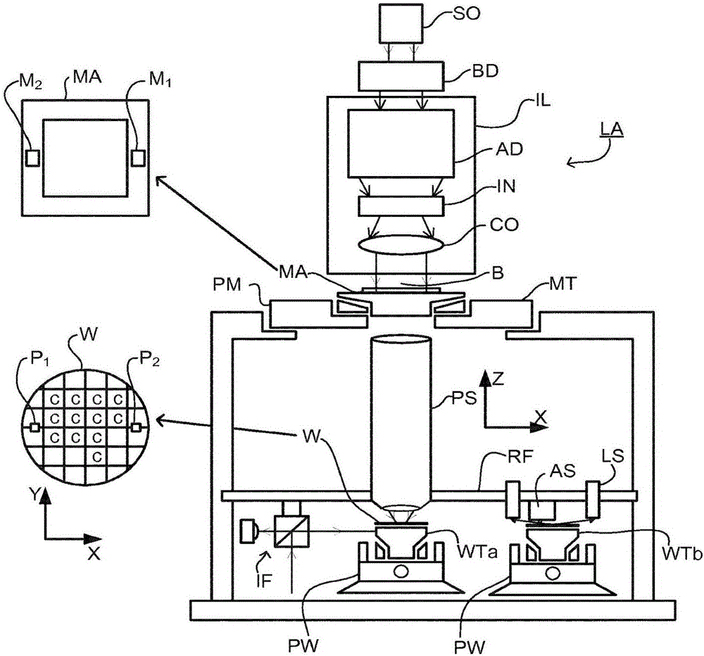
[0043] figure 1 A photolithographic setup is schematically shown. The unit includes:

[0044] - an illumination system (illuminator) IL configured to condition the radiation beam B (eg UV radiation or DUV radiation);

[0045] - a support structure (e.g. mask table) MT configured to support the patterning device (e.g. mask) MA and connected to a first positioner PM configured to position the pattern precisely according to certain parameters chemical equipment;

[0046] - a substrate table (e.g. wafer table) WT configured to hold a substrate (e.g. resist-coated wafer) W and connected to a second positioner PW configured to precisely parametrically position the substrate; and

[0047] - A projection system (eg a refractive projection lens system) PL configured to project the pattern imparted to the radiation beam B by the patterning device MA onto a target portion C of the substrate W (eg comprising one or more dies).

[0048] The illumination system may include various typ...


PUM


Abstract

The invention discloses an inspection apparatus, an inspection method and a device manufacturing method. The inspection apparatus (100) is used for measuring parameters of targets on a substrate. Coherent radiation follows an illumination path (solid rays) for illuminating target (T). A collection path (dashed rays) collects diffracted radiation from the target and delivers it to a lock-in image detector (112). A reference beam following a reference path (dotted rays). An acousto-optical modulator (108) shifts the optical frequency of the reference beam so that the intensity of radiation at the lock-in detector includes a time-varying component having a characteristic frequency corresponding to a difference between the frequencies of the diffracted radiation and the reference radiation. The lock-in image detector records two-dimensional image information representing both amplitude and phase of the time-varying component. A second reference beam with a different shift (110) follows a second reference path (dot-dash rays). Interference between the two reference beams can be used for intensity normalization.

Description

[0001] Cross References to Related Applications [0002] This application claims the benefit of EP Application 14176391 filed on 09.07.2014, the content of which is hereby incorporated by reference in its entirety. technical field [0003] The invention relates to an inspection device and an associated inspection method that can be used, for example, in the manufacture of devices by lithography. The invention also relates to methods of manufacturing devices and computer program products useful in implementing these methods. Background technique [0004] A lithographic apparatus is a machine that applies a desired pattern on a substrate, usually a target portion of the substrate. A lithographic apparatus may be used, for example, in the manufacture of integrated circuits (ICs). In this case, a patterning device (alternatively referred to as a mask or reticle) may be used to generate the circuit patterns to be formed on the respective layers of the IC. The pattern can be t...

Claims


Application Information

Patent Timeline
IPC IPC(8): G03F7/20
CPCG03F7/70625G03F7/70633G01N21/956G01J3/2823G01J3/45G01N21/4788G01N2201/06113G03F7/70491
Inventor A·辛格H·P·M·佩莱曼斯P·沃纳尔
Owner ASML NETHERLANDS BV
Why Eureka
Try Eureka