A Method for Analyzing Thermal Resistance of Nano-interface Bonding Layer of Microelectronic Devices

A technology of microelectronic devices and bonding layers, applied in instruments, electrical digital data processing, geometric CAD, etc., can solve problems such as the inability to test the thermal resistance of bonding layers at the nanometer interface, improve bonding quality, realize accurate characterization, The effect of improving the cooling capacity

Active Publication Date: 2020-08-07
NO 55 INST CHINA ELECTRONIC SCI & TECHNOLOGYGROUP CO LTD
View PDF3 Cites 0 Cited by
  • Summary
  • Abstract
  • Description
  • Claims
  • Application Information

AI Technical Summary

Problems solved by technology

[0004] The present invention proposes a method for analyzing the thermal resistance of the nano-interface bonding layer of a microelectronic device. The structural design of the layer sample is to meet the combination of laser flash test and thermal resistance numerical analysis, and realize the accurate characterization and quantitative analysis of the thermal resistance of the nano-scale interface layer, in order to improve the bonding quality of microelectronic devices and enhance their heat dissipation. The ability provides the basis for test analysis, solves the problem that the existing test methods cannot test the thermal resistance of the nano-interface bonding layer inside the microelectronic device, realizes the quantitative analysis of the thermal resistance of the nano-scale bonding layer, and contributes to the improvement of microelectronics The bonding quality of the device and the improvement of its heat dissipation capability provide the basis for test analysis

Method used


Image

  • A Method for Analyzing Thermal Resistance of Nano-interface Bonding Layer of Microelectronic Devices
  • A Method for Analyzing Thermal Resistance of Nano-interface Bonding Layer of Microelectronic Devices
  • A Method for Analyzing Thermal Resistance of Nano-interface Bonding Layer of Microelectronic Devices

Examples


Embodiment

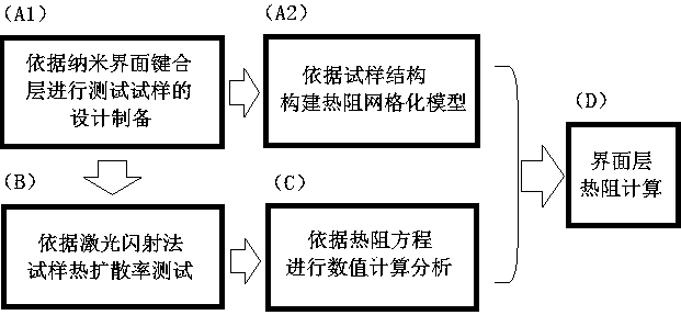
[0023] Thermal resistance analysis of benzocyclobutene (BCB) interfacial layer for wafer-level silicon-silicon bonding in microelectronic MEMS devices:

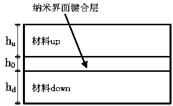
[0024] ①According to the actual size of the MEMS device wafer-level silicon-silicon bonded benzocyclobutene interface layer, design a three-layer test structure: Si-BCB-Si, the thickness of the upper layer of silicon and the thickness of the lower layer of silicon are equal to h u =h d =0.48mm, the thickness of the BCB nano bonding layer is 100nm; the test sample is prepared according to the design, and its plane size is Φ=12.7±0.05mm;

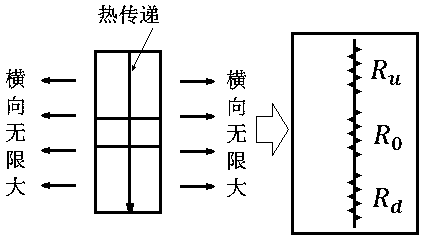
[0025] According to the design of Si-BCB-Si, the grid of the thermal resistance during the flash method test is carried out, that is, the heat in the heat transfer process first passes through the thermal resistance , and then through the thermal resistance , and finally through the thermal resistance , is a three-layer thermal resistance series structure, and the total thermal resist...


PUM

PropertyMeasurementUnit
thicknessaaaaaaaaaa
thicknessaaaaaaaaaa
diameteraaaaaaaaaa

Abstract

The invention relates to a method for analyzing the thermal resistance of a nano-interface bonding layer of a microelectronic device, comprising the following steps: (1) design and sample preparation of a test sample by a laser flash method containing a nano-interface bonding layer, and the thermal resistance of the sample Gridding; (2) The thermal diffusivity of the whole sample is obtained by laser thermal flash method, and the thermal resistance is calculated numerically in combination with the thermal resistance equation; (3) The thermal resistance of the nano-interface bonding layer is extracted by gridding thermal resistance analysis. The advantages of the present invention: 1) solve the problem that the existing testing method cannot test the thermal resistance of the nano-interface bonding layer inside the microelectronic device; The combination of numerical analysis of thermal resistance has recently realized the accurate characterization of the thermal resistance of the nanoscale interface layer; 3) The quantitative analysis of the thermal resistance of the nanoscale bonding layer of microelectronic devices has been realized, in order to improve its bonding quality and enhance its heat dissipation Capabilities provide the basis for test analysis.

Description

technical field [0001] The invention relates to a method for analyzing the thermal resistance of a nano-interface bonding layer of a microelectronic device, which is mainly applied to the research on the thermal characteristics of the nano-scale bonding layer of an electronic device. Background technique [0002] With the development of microelectronic devices towards systematization, integration, high power, and miniaturization, the heat flux inside the components continues to increase, which in turn leads to a decline in the performance and reliability of components. Studies have shown that about 55% of electronic components fail Mainly due to overheating and heat related issues. Therefore, the heat dissipation capability of components is becoming more and more important. As an important part of component packaging, the quality of the bonding layer and the dielectric material seriously affect the heat dissipation capability of the device. Especially in high-power-based d...

Claims


Application Information

Patent Timeline
Patent Type & Authority Patents(China)
IPC IPC(8): G06F30/17
CPCG06F30/17G06F30/333
Inventor 郭怀新吴立枢孔月婵陈堂胜
Owner NO 55 INST CHINA ELECTRONIC SCI & TECHNOLOGYGROUP CO LTD
Why Eureka
Try Eureka