Silicon through hole reliability analyzing method
An analysis method, the technology of through-silicon vias, applied in the field of microelectronics, can solve the problems of no consideration of stress, impossibility, idealization of the model, etc., and achieve the effect of wide application range
- Summary
- Abstract
- Description
- Claims
- Application Information
AI Technical Summary
Problems solved by technology
Method used
Image
Examples
Embodiment Construction
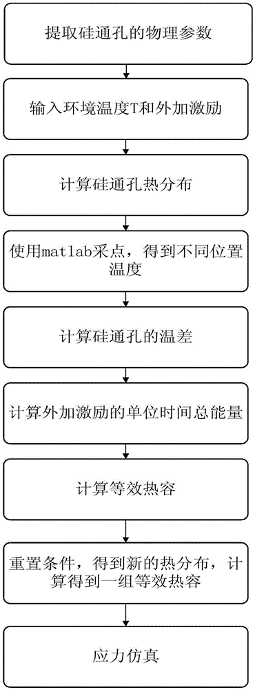
[0040] refer to figure 1 , the concrete realization of the present invention is as follows:
[0041] Step 1. Extract the physical parameters of the materials inside and outside the TSVs in the circuit.
[0042] Extract the physical parameters of the inner and outer layers of the TSV used in the circuit, the physical parameters include: the radius r of the upper surface of the TSV Cu1 , the lower surface radius r of the TSV Cu2 , the height H of the TSV, the resistance R of the copper pillar of the TSV, and the angle θ between the side surface and the bottom surface of the TSV 1 , r Cu1 Equal to the radius of the upper surface of the TSV copper pillar plus the thickness of the silicon dioxide on the upper surface of the TSV, r Cu2 It is equal to the radius of the lower surface of the TSV copper pillar plus the thickness of silicon dioxide on the lower surface of the TSV.
[0043] Step 2. Enter the ambient temperature T and external excitation used in the TSV.
[0044] Ent...
PUM
 Abstract
Description
Claims
Application Information


