Array substrate, display panel and display apparatus

An array substrate and array technology, applied in optics, instruments, electrical components, etc., can solve the problems of increased leakage current and inability to completely shield thin-film transistors, and achieve the effects of reducing leakage current and improving display performance

Active Publication Date: 2017-05-17
XIAMEN TIANMA MICRO ELECTRONICS
View PDF8 Cites 26 Cited by
  • Summary
  • Abstract
  • Description
  • Claims
  • Application Information

AI Technical Summary

Problems solved by technology

However, since the light-shielding layer usually only blocks the light that is vertically incident on the channel region of the active layer, the metal layers (such as the source-drain metal layer) of the thin film transistor and the stacked film layers with different refractive indices will reflect part of the light from the bottom backlight. , when the reflected light is incident on the channel re

Method used


Image

  • Array substrate, display panel and display apparatus
  • Array substrate, display panel and display apparatus
  • Array substrate, display panel and display apparatus

Examples


Example Embodiment

[0030] The application will be further described in detail below in conjunction with the accompanying drawings and embodiments. It should be understood that the specific embodiments described here are only used to explain related inventions, rather than to limit the invention. It should also be noted that, for the convenience of description, only the parts related to the related invention are shown in the drawings.

[0031] It should be noted that, in the case of no conflict, the embodiments in the present application and the features in the embodiments can be combined with each other. The present application will be described in detail below with reference to the accompanying drawings and embodiments.

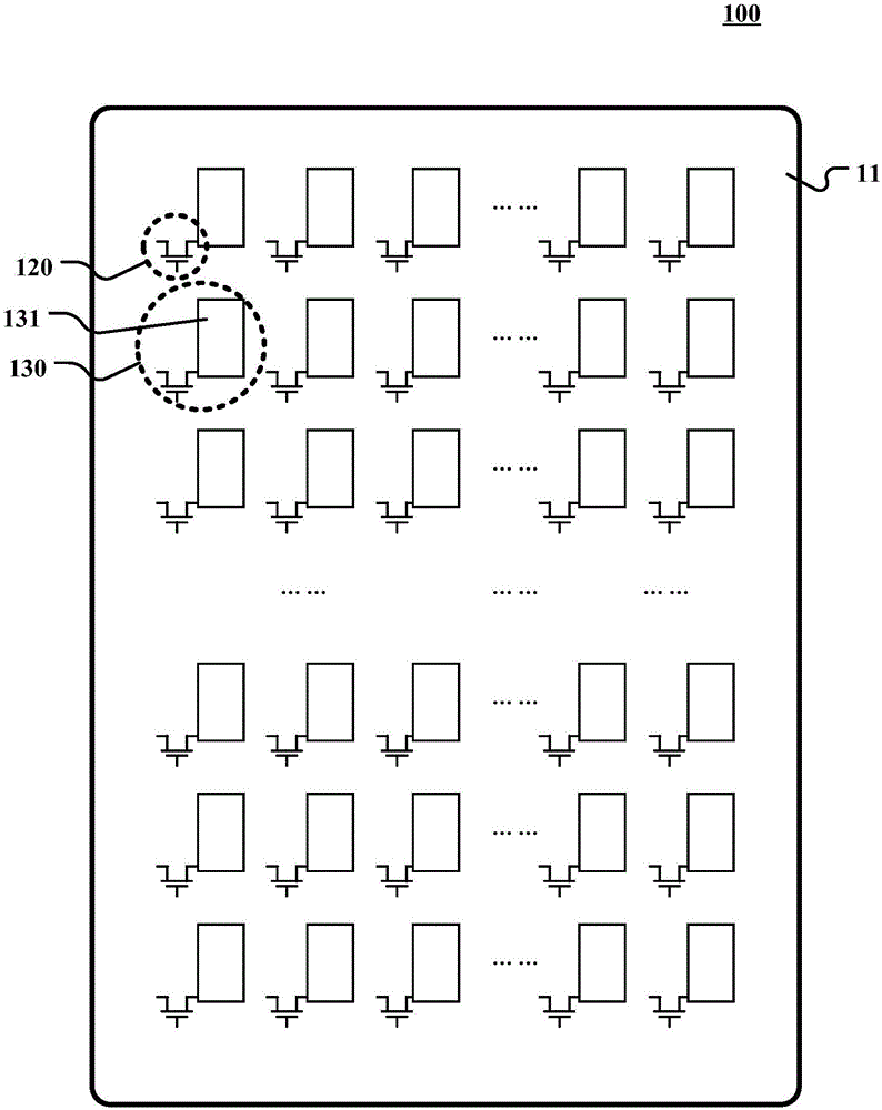
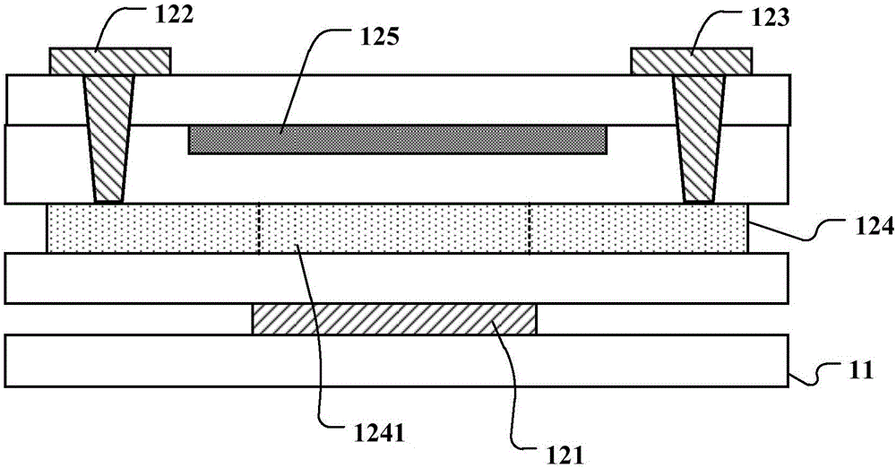
[0032] Please refer to figure 1 and figure 2 , which respectively show a schematic structural view and a schematic cross-sectional view of an embodiment of the array substrate provided in the embodiment of the present application.

[0033] like figure 1 As shown, the arr...


PUM

PropertyMeasurementUnit
Thicknessaaaaaaaaaa

Abstract

The invention discloses an array substrate, a display panel and a display apparatus. The array substrate comprises a substrate and a thin film transistor array positioned on the substrate, wherein a thin film transistor in the thin film transistor array comprises a source, a drain, a gate and an active layer; the active layer comprises a channel region which is controlled by the gate and formed between the source and the drain; the display panel comprises an optical barrier layer which is positioned on one side, far from the substrate, of the gate, and positioned on one side, far from the substrate, of the active layer; and the orthographic projection of the optical barrier layer towards the substrate covers that of the channel region towards the substrate. According to the scheme disclosed by the invention, the optical leakage current of the thin film transistor in the array substrate generated by illuminance on the active layer can be avoided, so that the display effect can be improved.

Description

technical field [0001] The present application relates to the field of display technology, in particular to an array substrate, a display panel and a display device. Background technique [0002] With the continuous expansion of the application field of the display technology, the requirement for the display performance is getting higher and higher. Usually, a display panel is provided with many thin film transistors (Thin Film Transistor, TFT), including a thin film transistor array disposed in a display area, and a thin film transistor disposed in a driving circuit in a non-display area. Most of these thin film transistors use monocrystalline silicon or polycrystalline silicon as the active layer. Since the silicon in the active layer will generate photocarriers under the irradiation of light, the leakage current of the thin film transistor device will increase when it is turned off, which will affect the display. performance, so it is necessary to block the light that hi...

Claims


Application Information

Patent Timeline
IPC IPC(8): H01L27/12H01L23/552G02F1/1335
CPCH01L23/552H01L27/1214G02F1/133512G02F1/133514
Inventor 刘博智吴晓晓
Owner XIAMEN TIANMA MICRO ELECTRONICS
Why Eureka
Try Eureka