Chip internal logic verify system and method

A technology of internal logic and verification system, applied in the field of electronics, can solve problems such as inevitable internal defects of products, affecting stable operation of the system, economic losses, etc., to achieve the effect of improving test efficiency and test coverage, saving test time, and reducing workload

Inactive Publication Date: 2017-05-24
BEIJING AEROSPACE AUTOMATIC CONTROL RES INST
View PDF4 Cites 7 Cited by
  • Summary
  • Abstract
  • Description
  • Claims
  • Application Information

AI Technical Summary

Problems solved by technology

Although chip manufacturers have been continuously improving the production process, it is theoretically inevitable that the product has internal defects
At the same time, the chip may also fail due to excessive vibration, extrusion and collision during transportation.
Once a defective chip is used in the circuit, it may affect the stable operation of the entire system, causing major liability accidents and serious economic losses

Method used


Image

  • Chip internal logic verify system and method
  • Chip internal logic verify system and method
  • Chip internal logic verify system and method

Examples


Embodiment Construction

[0034] In order to make the technical problems, technical solutions and advantages to be solved by the present invention clearer, the following will describe in detail with reference to the accompanying drawings and specific examples.

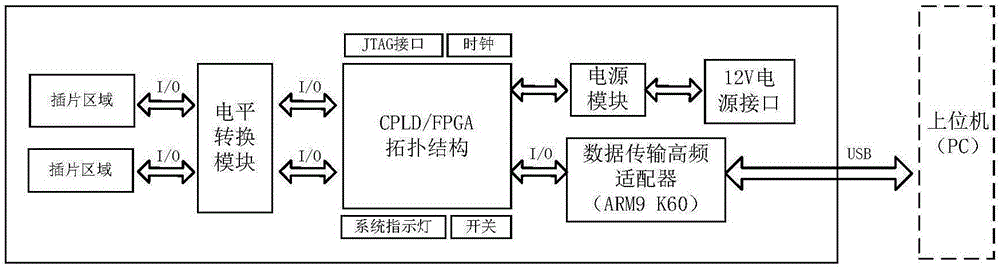
[0035] The principle of the embodiment of the present invention is: design through hardware platform design, utilize CPLD (programmable logic controller) and its peripheral circuit to simulate the internal input and output situation of the specified system, complete the configuration of I / O pulse signal, and load the excitation signal to The chip to be tested is to test some chips used by the specified system to judge whether its output logic is consistent with the standard output, so as to verify the correctness of the chip and ensure that the internal program files of the chip are correctly programmed and downloaded.

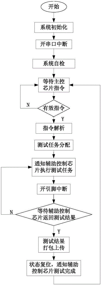
[0036] Such as figure 1 As shown, the internal logic verification system of the chip according to the embodiment of the prese...


PUM


Abstract

The invention provides a chip internal logic verify system characterized by comprising the following units: a main control module used for sending a control signal to a tested chip according to a control order and receiving a feedback signal of the tested chip; a level transition module used for carrying out level transition between the tested chip and the main control module; at least one I/O module used for connecting with the tested chip, wherein the I/O module is connected with the main control module through the level transition module. The system and method can test and verify the programmable chip internal logics; the chip internal logic verify system can test and verify chips in batch, thus reducing operation people workload, and improving testing efficiency and test coverage rate.

Description

technical field [0001] The invention relates to the field of electronic technology, in particular to a chip internal logic verification system and method. Background technique [0002] With the development of computer and network technology, the deep integration of industrialization and informatization has become an inevitable trend of technological development. In the modern integrated circuit manufacturing process, chip processing needs to go through a series of chemical, optical, metallurgical, thermal processing and other process links; each process may introduce various defects. Although chip manufacturers have been continuously improving the production process, it is theoretically inevitable that the product has internal defects. At the same time, the chip may also fail due to excessive vibration, extrusion and collision during transportation. Once a defective chip is used in the circuit, it may affect the stable operation of the entire system, causing major liabilit...

Claims


Application Information

Patent Timeline
Patent Type & Authority Applications(China)
IPC IPC(8): G01R31/3177
CPCG01R31/3177
Inventor 李鑫彭红五周饴然向刚
Owner BEIJING AEROSPACE AUTOMATIC CONTROL RES INST
Why Eureka
Try Eureka