System and method for thermal management of electronic devices

A technology for thermal management systems and electronic devices, which is applied in the direction of electrical components, electrical components, circuit heating devices, etc., and can solve problems such as increased parasitic capacitance, time-consuming, and manual assembly characteristics errors

Inactive Publication Date: 2017-05-24
TYCO HEALTHCARE GRP LP
View PDF10 Cites 5 Cited by
  • Summary
  • Abstract
  • Description
  • Claims
  • Application Information

AI Technical Summary

Problems solved by technology

[0004] Some of the disadvantages of hardware-mounted exposed chip semiconductor packages include: (1) additional mounting hardware is required to secure the device; (2) manual labor that may be required to assemble the mechanical hardware may incur additional component and assembly costs; (3) manual assembly characteristics that may be prone to error; (4) when a common heat sink is used for multiple semiconductor devices, devices with different voltages on their corresponding exposed pads must be electrically insulated from the heat sink and/or from each other; and (5) device repair and/or or replacing can be time consuming
Furthermore, the use of large circuit board copper planes or large external heat sinks that are electrically connected to the semiconductor to con

Method used


Image

  • System and method for thermal management of electronic devices
  • System and method for thermal management of electronic devices
  • System and method for thermal management of electronic devices

Examples


Embodiment Construction

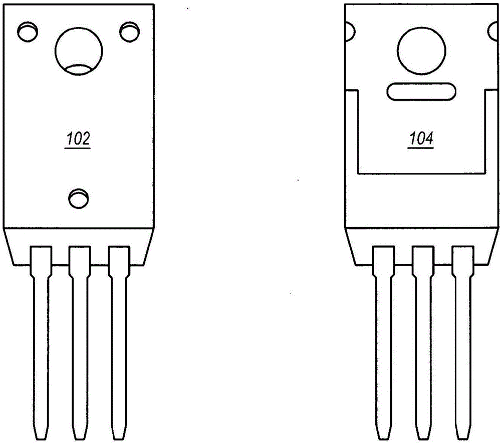
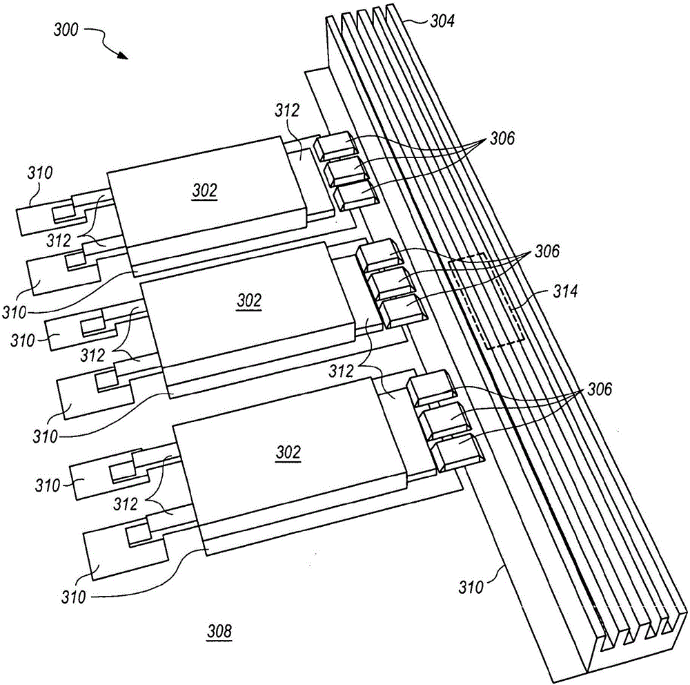
[0035] image 3 A diagram of a thermal management system 300 for an electronic device is shown. System 300 includes one or more electronic components 302 , a heat sink 304 , and one or more thermally conductive and electrically insulating thermal bridges 306 . In one example, semiconductor device 302 is a power field effect transistor (FET) or other device that generates heat during operation that must be conducted away from the device to manage device temperature so that it remains within normal operating limits.

[0036] Each thermal bridge 306 is between the heat sink 304 and a corresponding one of the electronic devices 302, thermally couples a corresponding one of the electronic devices 302 to the heat sink 304, and electrically connects a corresponding one of the electronic devices 302 to the heat sink 304. insulation. In one example, multiple thermal bridges (three thermal bridges in the example system 300 ) are interposed between the heat sink 304 and a respective one o...


PUM


Abstract

A thermal management system and method for electronic devices is provided. The system includes an electronic device, a heat sink, and a thermally conducting and electrically insulating thermal bridge that is interposed between the electronic device and the heat sink. The thermal bridge thermally couples the electronic device to the heat sink and electrically isolates the electronic device from the heat sink. The electronic device, the heat sink, and the thermal bridge are mounted on a same planar surface of a printed circuit board.

Description

technical field [0001] This application relates to electronic circuits. More specifically, the present application relates to thermal management systems and methods for electronic devices. Background technique [0002] Semiconductors such as transistors and diodes are sometimes fabricated in semiconductor packages where mechanical mounting is combined with electrical connections. An example of a top view 102 and a bottom view 104 of such a package, sometimes referred to as an exposed tab package, is shown in FIG. 1 . Exposed chip semiconductor packages are sometimes used as an alternative to hermetic packages because exposed chip packages can exhibit better heat transfer capabilities, power handling capabilities, and current handling capabilities than hermetic semiconductor packages. Chipless semiconductor packages are available in at least two configurations, one as shown in Figure 1 designed to be mounted using mechanical hardware such as screws, nuts, and / or insulators,...

Claims


Application Information

Patent Timeline
IPC IPC(8): H05K7/20
CPCH05K7/2039H05K7/205H01L23/36H01L23/3672H01L23/3731H01L23/40H05K1/0209H05K2201/066H05K2201/10151H05K1/0203H05K1/0213H05K13/0486H05K2201/06
Inventor S·C·拉普D·A·弗里德里克斯R·B·史密斯
Owner TYCO HEALTHCARE GRP LP
Why Eureka
Try Eureka