FPGA transistor size adjustment method

An adjustment method and transistor technology, applied in the field of FPGA architecture exploration, can solve problems such as reducing the efficiency of architecture exploration, and achieve the effects of reducing the amount of training data, fast transistor size adjustment, and accurate results

Inactive Publication Date: 2017-05-31
TIANJIN UNIV
View PDF2 Cites 5 Cited by
  • Summary
  • Abstract
  • Description
  • Claims
  • Application Information

AI Technical Summary

Problems solved by technology

However, the use of circuit simulators still reduces the efficiency of architecture exploration

Method used


Image

  • FPGA transistor size adjustment method
  • FPGA transistor size adjustment method
  • FPGA transistor size adjustment method

Examples


Embodiment Construction

[0029] The present invention provides an accurate transistor size adjustment method, which can quickly find a result that meets the design target under the requirement of a large number of design iterations, and the finally obtained optimization result can be applied to an architecture exploration tool to speed up the architecture exploration process. The specific technical scheme is as follows:

[0030] 1) Determine the key parameters that affect the FPGA delay.

[0031] 2) According to the impact of parameters on the delay of each sub-circuit in the FPGA, a corresponding Elmore delay model is established for each circuit.

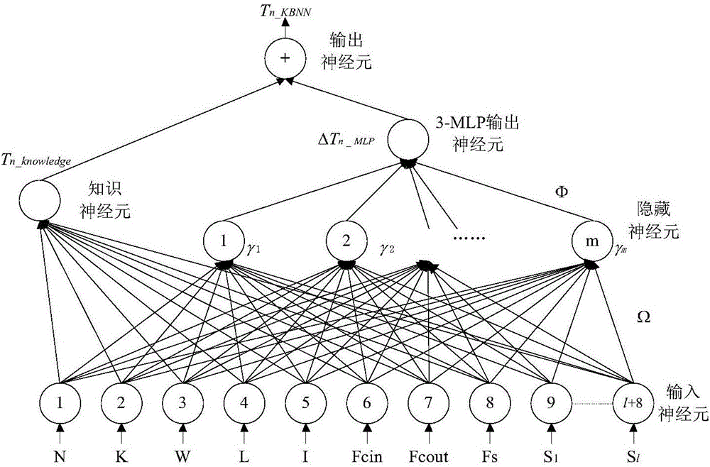
[0032] 3) Combine the Elmore delay model of FPGA with the neural network to establish the KBNN delay model and train it to determine the training error E t and validation error E v Minimum weights Ω and Φ and number of hidden neurons m.

[0033] 4) Establish an improved minimum-width transistor area model to estimate the area of ​​the FPGA island.

[...


PUM


Abstract

The invention relates to an FPGA architecture exploration method. The method aims at combining a precise model with a GA algorithm, and achieves trade-off optimization between delay and area by adjusting size of the transistor. To achieve the goal, the FPGA architecture exploration method comprises the following steps of (1) determining key parameters that affects the delay of the FPGA; (2) establishing corresponding ELmore delay model for each circuit; (3) combining the Elmore delay model of the FPGA with a nerve net, establishing a KBNN delay model, conducting training to the KBNN delay model, determining a weight omega and phi that minimize a training error Et and a verification error Ev, and the number of hidden neurons m; (4) establishing an improved minimum width transistor area model, and estimating the area of the FPGA island; (5) combining the delay model, the area model and the GA algorithm, achieving fast adjustment of the size of the transistor. The method is mainly applied to an FPGA design occasion.

Description

technical field [0001] The invention relates to a method for exploring an FPGA architecture, in particular to a method for adjusting the size of an FPGA transistor. Background technique [0002] In the field-programmable gate array FPGA (Field-Programmable Gate Array) architecture exploration process, transistor-level design tools are essential, because it can provide accurate delay and area estimates for different architectures, so as to realize the evaluation of the architecture . Transistor-level design involves choosing circuit topologies for different subcircuits to enable architectural choices. Transistor sizing can also improve FPGA area, latency, and power consumption. FPGA design is a complex iterative process of transistor-level design for different architectures. To obtain correct transistor sizing results, accurate delay and area models are essential. [0003] Currently, there are three methods that can be used to estimate the delay of FPGA. In the first met...

Claims


Application Information

Patent Timeline
Patent Type & Authority Applications(China)
IPC IPC(8): G06F13/42
CPCG06F13/42
Inventor 钱涵晶刘强
Owner TIANJIN UNIV
Why Eureka
Try Eureka