Method for manufacturing third-generation image intensifier by using gallium arsenide wafer

A technology of image intensifier and gallium arsenide crystal, which is applied in the field of making third-generation image intensifiers using gallium arsenide wafers, can solve the problems that the product qualification rate is only 40%, the input and income are not proportional, and the air is not easy to be completely eliminated. Strong practical value, low cost, and low probability of occurrence

Inactive Publication Date: 2017-05-31
BEIJING HANYUANYINUO TECH
View PDF4 Cites 0 Cited by
  • Summary
  • Abstract
  • Description
  • Claims
  • Application Information

AI Technical Summary

Problems solved by technology

[0004] 1. This method has higher requirements on the atmospheric pressure in the ultra-high vacuum chamber, which needs to be lower than 10 -11 Pascal can work normally, therefore, the time required for the degassing process of the vacuum chamber is long, resulting in low product production efficiency;
[0005] 2. Using this method, the air in the vacuum chamber is not easy to be completely removed. When the indoor temperature is increased, the remaining oxygen molecules, oxygen-containing gas and water vapor will react chemically with the surface of

Method used


Image

  • Method for manufacturing third-generation image intensifier by using gallium arsenide wafer
  • Method for manufacturing third-generation image intensifier by using gallium arsenide wafer

Examples


Embodiment Construction

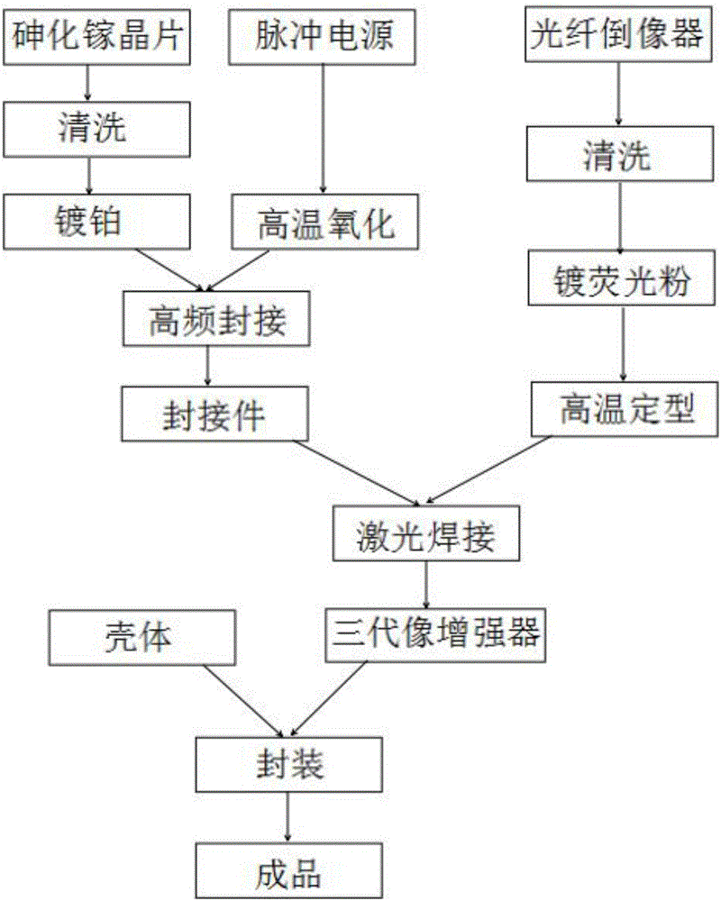
[0029] The present invention will be further described in detail below in conjunction with the accompanying drawings and specific embodiments.

[0030] Such as figure 1 , figure 2 Shown, overall steps of the present invention are as follows:

[0031] One: Clean the gallium arsenide wafer, and then plate a conductive layer to make the resistance reach the rated standard;

[0032] First of all, when the cleanliness is greater than 100 and the vacuum degree is greater than 10 -5 GaAs wafers are ultrasonically cleaned in the clean room of Pa, so that the clean room standard meets the environmental requirements of vacuum device process cleanliness; strictly following the clean room work requirements and maintaining its cleanliness is the basic guarantee for making image intensifiers. Ultrasonic cleaning is effective in loosening strongly bonded contaminants on the surface of GaAs wafers.

[0033] According to the different types of pollutants, pure water or organic solvent cle...


PUM

PropertyMeasurementUnit
Thicknessaaaaaaaaaa
Resistanceaaaaaaaaaa

Abstract

The invention discloses a method for manufacturing a third-generation image intensifier by using a gallium arsenide wafer. The method comprises the steps of performing ultrasonic wave cleaning on the gallium arsenide wafer firstly, and then plating a platinum conductive layer; performing ultrasonic wave cleaning on the platinum-plated gallium arsenide wafer again, and performing high-frequency sealing and packaging with a high-temperature oxidized pulse power supply to form a sealing part; next, performing laser welding on an optical fiber image inverter which is subjected to cleaning, fluorescent powder coating and high-temperature shaping in sequence, and the sealing part to further form a core assembly; and performing packaging on the core assembly and a shell to complete the manufacturing. The production link is subjected to process control, so that the method is applicable to batch production, high in production efficiency, low in side reaction, and high in percent of pass of products; the used device or equipment can be purchased from the market, so that the cost is low and market monopoly can be broken; and in addition, the third-generation image intensifier is relatively long in service life and the service life can be prolonged from 10,000 hours as a common image intensifier to 30,000 hours.

Description

technical field [0001] The invention relates to a manufacturing method, in particular to a method for manufacturing a third-generation image intensifier using a gallium arsenide wafer. Background technique [0002] The commonly used manufacturing method of the third-generation image intensifier is: regularly send the fluorescent screen assembly into the ultra-high vacuum chamber through the loading gate chamber, carry out airtight degassing and electron bombardment cleaning, and then send it into the assembly ultra-high vacuum chamber; The photocathode assembly is sent into the ultra-high vacuum chamber through the loading gate chamber for airtight pre-degassing; then the photocathode assembly is sent to the adjacent ultra-high vacuum chamber for batch final cleaning and sensitization treatment, and the photocathode is formed and sent to assembly Ultra-high vacuum chamber: In the assembly ultra-high vacuum chamber, the photocathode and fluorescent screen components are assem...

Claims


Application Information

Patent Timeline
IPC IPC(8): H01J9/00H01J9/12H01J31/50
CPCH01J9/00H01J9/12H01J31/50
Inventor 王坤
Owner BEIJING HANYUANYINUO TECH
Why Eureka
Try Eureka