Measuring Method of Sheet Resistance in Ohmic Contact Area Based on Vertical Test Pattern
A technology of ohmic contact area and test pattern, which is applied in the field of microelectronics to achieve the effect of improving performance and reliability, simple test method and simple test pattern
- Summary
- Abstract
- Description
- Claims
- Application Information
AI Technical Summary
Problems solved by technology
Method used
Image
Examples
Embodiment Construction
[0034] The specific implementation of the present invention will be further described in detail below in conjunction with the accompanying drawings and examples. The following examples are used to illustrate the present invention, but are not intended to limit the scope of the present invention.
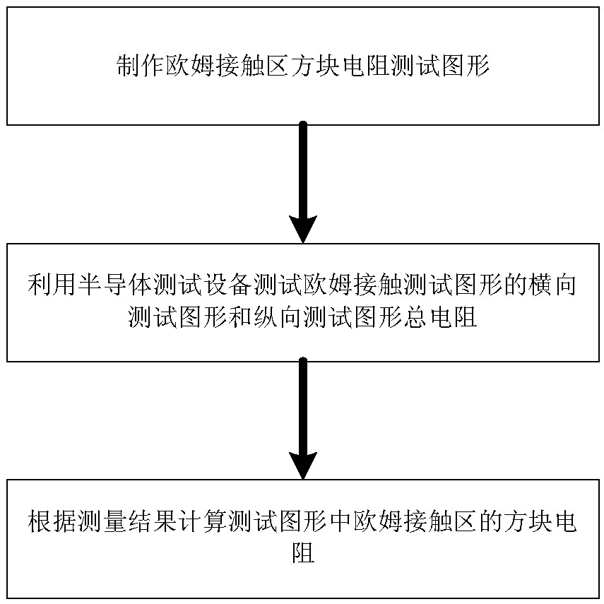
[0035] refer to figure 1 , the present invention carries out the step of ohmic contact area sheet resistance test as follows:
[0036] Step 1, make the test pattern of the square resistance in the ohmic area.
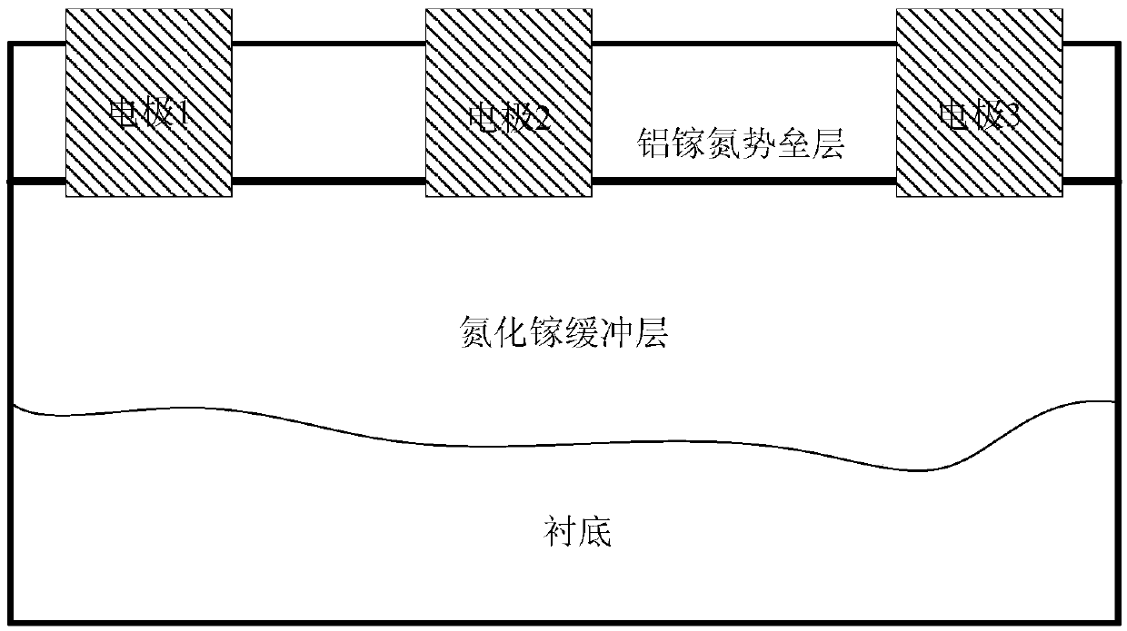
[0037] refer to figure 2 , this step prepares the test pattern of the sheet resistance of the ohmic contact area according to the cross-sectional structure of the existing test pattern, and the steps are as follows:
[0038] 1a) Setting the structure of the test pattern: it is a substrate layer, a GaN buffer layer and an AlGaN barrier layer from bottom to top;
[0039] 1b) Depositing a metal electrode on the AlGaN barrier layer material;
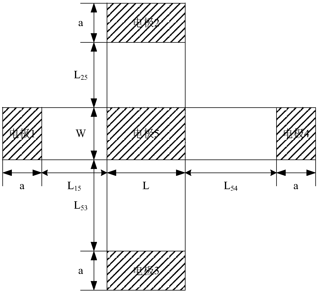
[0040] 1c) Prepare a set of tra...
PUM
 Abstract
Description
Claims
Application Information


