
SiC JFET device for integrating schottky diode and making method thereof

A technology for Schottky diodes and a manufacturing method, which is applied in semiconductor/solid-state device manufacturing, electric solid-state devices, semiconductor devices, etc., can solve the problems of difficulty in controlling the channel width threshold voltage consistency, high process difficulty, etc., and achieve increased power Density and reliability, the effect of reducing size and cost

Pending Publication Date: 2017-05-31
BEIJING CENTURY GOLDRAY SEMICON CO LTD
View PDF6 Cites 13 Cited by
  • Summary
  • Abstract
  • Description
  • Claims
  • Application Information

AI Technical Summary

Problems solved by technology

The process of the trench structure JFET is relatively difficult, especially the etching of the trench, the control of the channel width, and the resulting consistent control of the threshold voltage are very difficult.

Method used


Image

  • SiC JFET device for integrating schottky diode and making method thereof
  • SiC JFET device for integrating schottky diode and making method thereof
  • SiC JFET device for integrating schottky diode and making method thereof

Examples


Embodiment Construction

[0050] The present invention will now be described more fully with reference to the accompanying drawings, in which exemplary embodiments of the invention are shown. This invention may, however, be embodied in many different forms and should not be construed as limited to the exemplary embodiments set forth herein. Rather, these embodiments are provided so that this disclosure will be thorough and complete, and will fully convey the scope of the invention to those skilled in the art.

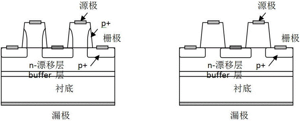
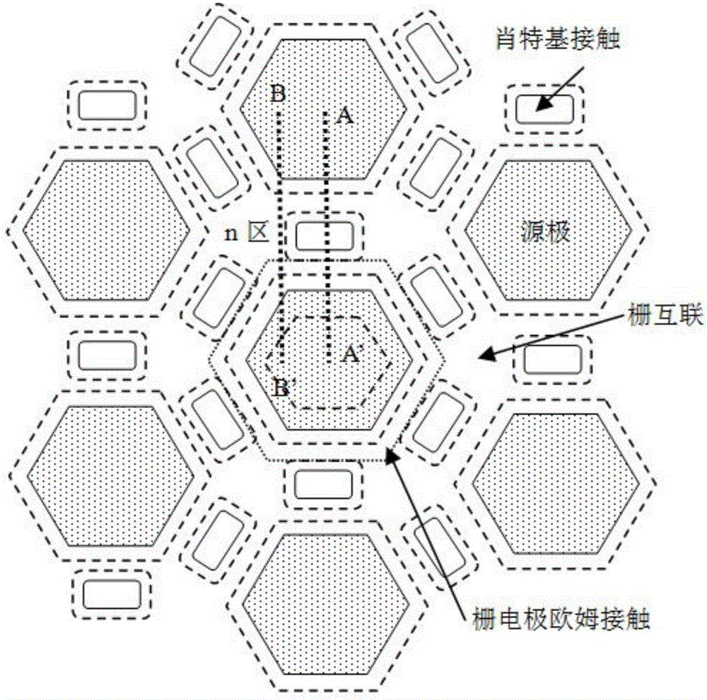
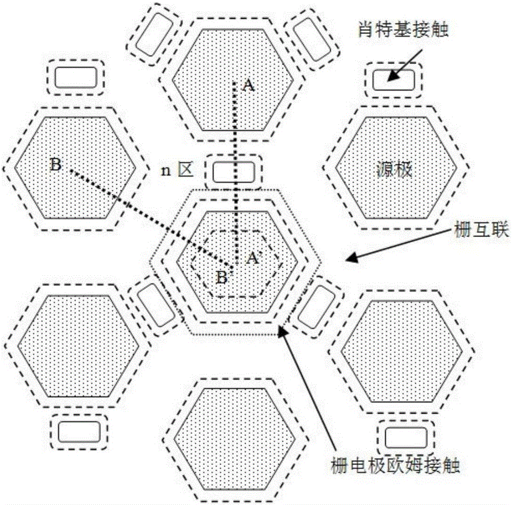
[0051] Such as Figure 2a , 2b , 2c, 3a, 3b and 3c, the present invention provides a SiC JFET device with integrated Schottky diode, the original cell structure of the active region of the SiC JFET device is drain, SiC substrate, buffer layer, n-drift layer, two p+ well layers symmetrically arranged left and right, n channel layer, p+ region, n++ region, p+ region, p+ region, n++ region and p+ region arranged symmetrically from left to right, from The source, gate, Schottky contact, gate and ...


PUM


Abstract

The invention discloses a SiC JFET (junction type field effect transistor) device for integrating a schottky diode. A primitive cell structure of the SiC JFET device for integrating the schottky diode in an active region from bottom to top successively comprises a drain electrode, a SiC substrate, a buffer layer, an n-drifting layer, two p+ trap layers arranged in bilateral symmetry, an n channel layer, and two p+ regions arranged in bilateral symmetry on the two sides of the n channel layer; a p+ region, a n++ region, the p+ region, the n++ region and another p+ region are successively arranged from left to right in symmetry; a source electrode, a grid electrode, a schottky contact, another grid electrode and another source electrode are successively arranged from left to right in symmetry; the source electrode is arranged on the p+ region and the n++ region, adjacent to the left and right sides of the primitive cell structure, the grid electrode is arranged on the middle p+ region on the left and right sides of the primitive cell structure, the schottky contact is arranged on a partial middle n region of the primitive cell structure in the active region, and no schottky contact is arranged on other parts of the n region of the primitive cell structure. The SiC JFET device that integrates JFET and V JFET into one, and integrates a schottky diode is disclosed. In addition, a making method is provided.

Description

technical field [0001] The invention belongs to the field of semiconductors, and in particular relates to a SiC JFET device integrating Schottky diodes and a manufacturing method thereof. Background technique [0002] Compared with SiC MOSFET, which is affected by the performance and reliability of the gate dielectric, SiC JFET has higher robustness because it has no MOS gate structure. It has been reported that SiC JFETs can function normally for 10,000 hours at a junction temperature of 500°C. This is the highest report on high-temperature applications of SiC and even wide-bandgap semiconductor power devices, reflecting the extremely superior high-temperature resistance of SiC devices. In contrast, high-temperature applications for MOSFETs have not yet exceeded 250°C. [0003] At present, there are two kinds of JFETs that are more common, the LJFET of the lateral channel and the VJFET of the vertical channel. Because LJFET is a lateral channel device, it is not suitable...

Claims


Application Information

Patent Timeline
IPC IPC(8): H01L27/07H01L29/10H01L29/78H01L29/808H01L21/8232
CPCH01L27/0705H01L29/1058H01L29/78H01L29/808H01L29/8083H01L21/8232
Inventor 倪炜江
Owner BEIJING CENTURY GOLDRAY SEMICON CO LTD
Features
  • Generate Ideas
  • Intellectual Property
  • Life Sciences
  • Materials
  • Tech Scout
  • Unparalleled Data Quality
  • Higher Quality Content
  • 60% Fewer Hallucinations
Learn More