

Thin film transistor, fabrication method thereof, display substrate and display device
A technology of a thin film transistor and a manufacturing method, which are applied in the fields of thin film transistors and their manufacturing methods, display devices, and display substrates, can solve the problems of metal oxide thin film transistor stability effects, damage to the back channel, etc., and achieve shortening of etching time, The effect of reducing damage and improving stability
- Summary
- Abstract
- Description
- Claims
- Application Information
AI Technical Summary
Problems solved by technology
Method used
Image

Examples
Embodiment 1
[0052] This embodiment provides a method for manufacturing a thin film transistor, including:
[0053] Forming a metal oxide semiconductor pattern, the metal oxide semiconductor pattern includes a first metal oxide semiconductor layer and a second metal oxide semiconductor layer stacked, the second metal oxide semiconductor layer is located on the first metal oxide semiconductor layer Above the material semiconductor layer;
[0054] Depositing a source and drain metal layer on the metal oxide semiconductor pattern, etching the source and drain metal layer and the second metal oxide semiconductor layer to form a source electrode, a drain electrode and an active layer of a thin film transistor, Wherein, the active layer is obtained after removing the second metal oxide semiconductor layer between the source electrode and the drain electrode with a first etchant, and the first etchant does not affect the second metal oxide semiconductor layer. The etching rate of the second meta...
Embodiment 2
[0093]Below in conjunction with accompanying drawing, the manufacturing method of thin film transistor of the present invention is further introduced:
[0094] The manufacturing method of the thin film transistor of the present embodiment comprises the following steps:
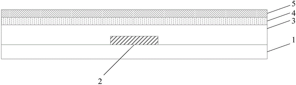
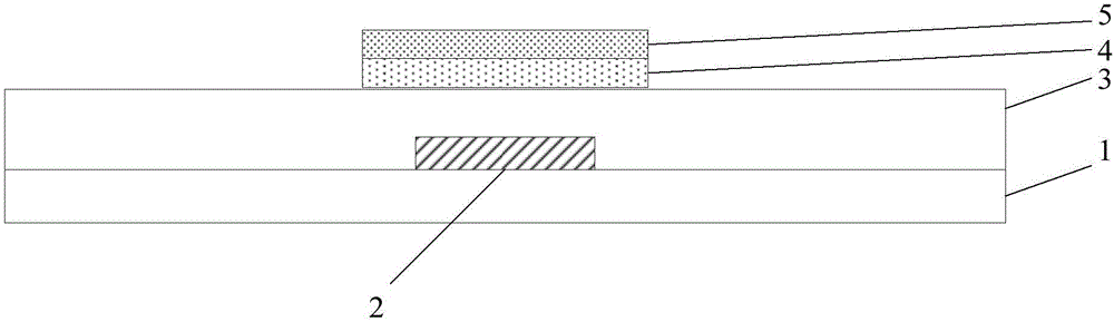
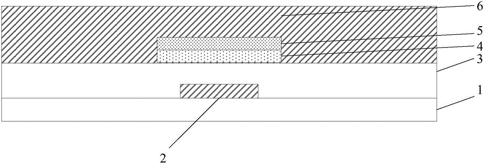
[0095] Step 1: If figure 1 As shown, a gate electrode 2, a gate insulating layer 3, a first metal oxide semiconductor layer 4 and a second metal oxide semiconductor layer 5 are formed on a base substrate 1;
[0096] Wherein, the base substrate 1 may be a glass substrate or a quartz substrate. Specifically, sputtering or thermal evaporation can be used to deposit a thickness of about The gate metal layer, the gate metal layer can be Cu, Al, Ag, Mo, Cr, Nd, Ni, Mn, Ti, Ta, W and other metals and alloys of these metals, the gate metal layer can be single-layer structure or multi-layer Structure, multi-layer structure such as Cu\Mo, Ti\Cu\Ti, Mo\Al\Mo, etc. A layer of photoresist is coated on the gate metal l...
Embodiment 3
[0108] Below in conjunction with accompanying drawing, the manufacturing method of thin film transistor of the present invention is further introduced:
[0109] The manufacturing method of the thin film transistor of the present embodiment comprises the following steps:
[0110] Step 1: If figure 1 As shown, a gate electrode 2, a gate insulating layer 3, a first metal oxide semiconductor layer 4 and a second metal oxide semiconductor layer 5 are formed on a base substrate 1;
[0111] Wherein, the base substrate 1 may be a glass substrate or a quartz substrate. Specifically, sputtering or thermal evaporation can be used to deposit a thickness of about The gate metal layer, the gate metal layer can be Cu, Al, Ag, Mo, Cr, Nd, Ni, Mn, Ti, Ta, W and other metals and alloys of these metals, the gate metal layer can be single-layer structure or multi-layer Structure, multi-layer structure such as Cu\Mo, Ti\Cu\Ti, Mo\Al\Mo, etc. A layer of photoresist is coated on the gate metal ...
PUM
 Abstract
Description
Claims
Application Information