Epitaxial growth method for improving quality of LED
A technology of light-emitting diodes and epitaxial growth, applied in electrical components, circuits, semiconductor devices, etc., can solve the problems of high stress on the light-emitting layer and low luminous efficiency of the light-emitting layer, achieve stress relief, improve electrical parameters and light efficiency, improve The effect of LED quality
- Summary
- Abstract
- Description
- Claims
- Application Information
AI Technical Summary
Problems solved by technology
Method used
Image

Examples
Embodiment 1
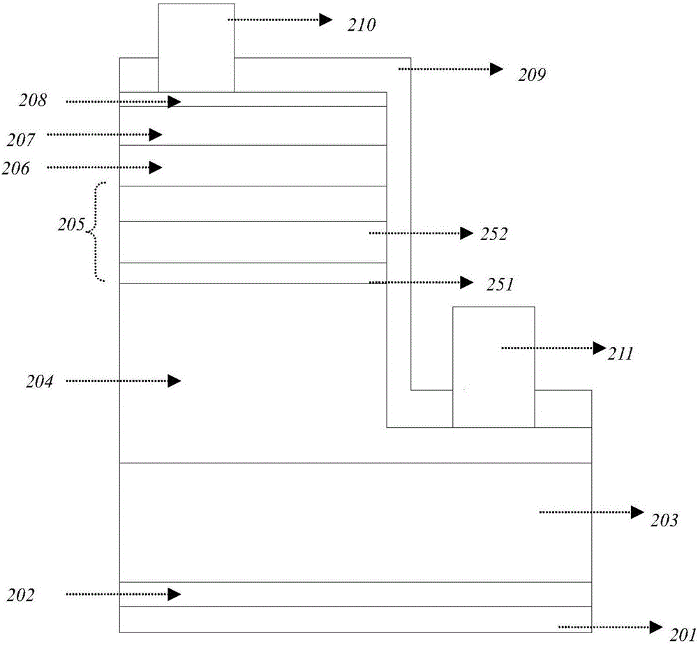
[0062] Such as Figure 4 As shown, it is a schematic structural diagram of the light-emitting diode described in the embodiment of the present invention. The structure of the light-emitting diode described in the present embodiment includes: the substrate sapphire Al 2 o 3 Layer 401, low temperature buffer layer GaN layer 402, undoped GaN layer 403, Si-doped GaN layer 404, stress release layer 405 (including: SiInN layer 451, SiInGaN layer 452), light emitting layer 406 (including: In x Ga (1-x) N layer 461, GaN layer 462), P-type AlGaN layer 407, Mg-doped P-type GaN layer 408, ITO layer 409, SiO 2 protective layer 410 , P electrode 411 , and N electrode 412 .
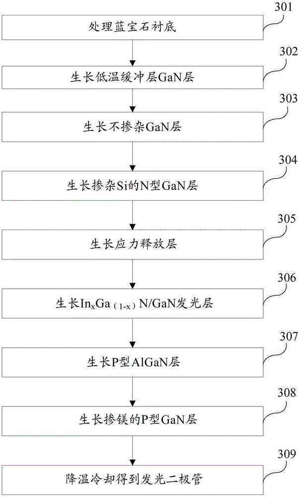
[0063] image 3 It is a schematic flow chart of the epitaxial growth method for improving the quality of light-emitting diodes described in this embodiment; the method described in this embodiment solves the technical problem of low luminous efficiency of the light-emitting layer caused by high stress in the light-...
Embodiment 2
[0077] Figure 6 It is a schematic flow chart of the epitaxial growth method for improving the quality of light-emitting diodes described in the embodiment of the present invention; this embodiment further describes the epitaxial growth method of light-emitting diodes on the basis of embodiment 1. The epitaxial growth method for improving the quality of light-emitting diodes described in this embodiment includes the following steps:
[0078] Step 601, at a temperature of 1000-1100°C, inject 100L / min-130L / min of H 2 1. The sapphire substrate is processed for 8-10 minutes under the condition that the pressure of the reaction chamber is kept at 100-300 mbar.
[0079] Step 602, lower the temperature to 500-600°C, keep the reaction chamber pressure at 300-600mbar, and feed NH at a flow rate of 10000-20000sccm 3 , 50-100sccm TMGa, 100L / min-130L / min H 2 , grow a low-temperature buffer GaN layer with a thickness of 20-40nm on a sapphire substrate.
[0080] Step 603, raise the temp...
Embodiment 3
[0094] The application examples of the epitaxial growth method for improving the quality of light-emitting diodes of the present invention are provided below, and a comparison test is carried out between the prior art preparation method of LED and the preparation method of the above-mentioned examples, as shown in Table 1:
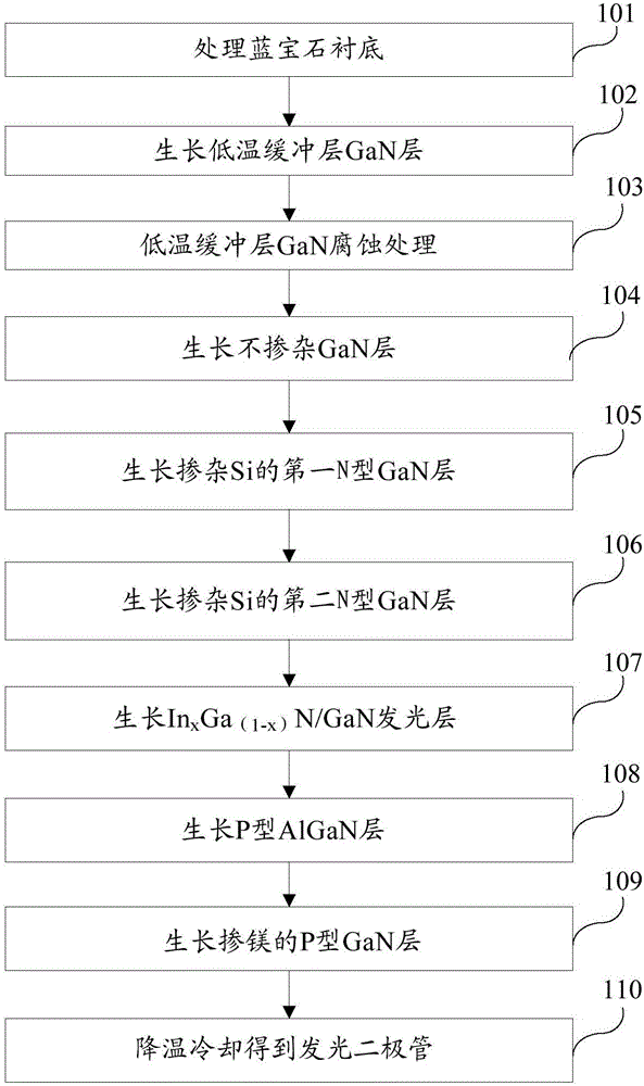
[0095] Sample 1 is an LED prepared by the prior art, and the preparation process is as follows figure 1 Shown; Sample 2 is the LED prepared by this patented technology, and the preparation process is as follows image 3 As shown; the difference between the sample 1 and sample 2 light-emitting diode epitaxial growth methods lies in: the growth conditions of the light-emitting layer are different. The comparative experiment of sample 1 and sample 2's photoelectric performance is as follows: Figure 5 As shown, the steps are as follows:
[0096] In step 501, take three LED samples of the prior art LED sample 1 and the LED sample 2 of the inventive technolo...
PUM
 Abstract
Description
Claims
Application Information