Semiconductor optical amplifier

An optical amplifier and semiconductor technology, used in semiconductor lasers, lasers, laser parts, etc., can solve the problems of low optical gain saturated optical output power, inability to achieve miniaturization, small mode volume, etc., and achieve compression divergence angle, photon density, etc. The effect of increasing, increasing the pattern volume

Active Publication Date: 2017-05-31
CHANGCHUN UNIV OF SCI & TECH
View PDF5 Cites 8 Cited by
  • Summary
  • Abstract
  • Description
  • Claims
  • Application Information

AI Technical Summary

Problems solved by technology

At present, semiconductor optical amplifiers have problems such as small mode volume, low optical gain, and low saturated optical output power. Using an array of multiple straight waveguide semiconductor optical amplifiers, the power can be increased through photopolymerization, but this structure requires external optical components. Photopolymerization cannot meet miniaturization requirements

Method used


Image

  • Semiconductor optical amplifier

Examples


Embodiment Construction

[0008] The technical solutions of the present invention will be described in further detail below with reference to the accompanying drawings and embodiments.

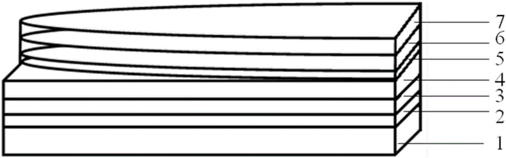
[0009] The present invention proposes a GaAs-based semiconductor optical amplifier with a parabolic curved waveguide. The structure of the semiconductor optical amplifier consists of a substrate, an N-type buffer layer, an N-type lower confinement layer, an N-type lower waveguide layer, a quantum well active region, The P-type upper waveguide layer and the P-type upper confinement layer are composed of the P-type waveguide layer with a parabolic curved surface structure, and the N-type GaAs substrate and the N-type Al x Ga 1- x As buffer layer, N-type AlGaAsSb lower confinement layer, N-type Al x Ga 1-x As lower waveguide layer, In x Ga 1-x As quantum well active region, P-type Al x Ga 1-x A semiconductor optical amplifier with a waveguide layer on an As parabolic curved surface structure and a confinement layer...


PUM


Abstract

The invention discloses a semiconductor optical amplifier, and especially relates to a GaAs-based semiconductor optical amplifier having a parabola-shaped curved-surface waveguide structure. Material of the semiconductor optical amplifier is a GaAs-based material system. An N-type AlxGa1-xAs buffer layer, an N-type AlGaAsSb lower limit layer, an N-type N-AlxGa1-xAs lower waveguide layer, an InxGa1-xAs quantum well active region, a P-type AlxGa1-xAs upper waveguide layer and a P-type AlGaAsSb upper limit layer are epitaxially prepared on an N-type GaAs substrate in sequence. The upper waveguide layer of the semiconductor optical amplifier is in the parabola-shaped curved-surface structure; such structure can enable a parabola-shaped curved-surface tip to have higher photon density, thereby improving mode volume of the semiconductor optical amplifier and enabling the semiconductor optical amplifier to have higher gain; and meanwhile, the parabola-shaped curved-surface waveguide structure facilitates compressing divergence angle of the semiconductor optical amplifier, thereby realizing high-power output and improving fiber coupling efficiency. The parabola-shaped curved-surface structure of the upper waveguide layer of the semiconductor optical amplifier is prepared through electron beam lithography or ultra-violet lithography, and then, through a dry method and wet method combined etching process.

Description

technical field [0001] The invention relates to the field of semiconductor optical amplifiers, in particular to a GaAs-based semiconductor optical amplifier with a parabolic curved surface waveguide structure. Background technique [0002] A semiconductor optical amplifier is an optoelectronic device that uses semiconductor materials as a gain medium to amplify or provide gain to external photons. It has a large operating wavelength range, simple structure, small size, and low power consumption. Devices are mixed or monolithically integrated, and the manufacturing process is mature. The semiconductor optical amplifier is an important device to realize all-optical signal processing and compensate optical loss in the future all-optical network. It has a wide range of applications in optical communication systems. It can be used as the preamplifier and optical split compensation amplifier of the machine, and can also be used as a nonlinear device for optical signal processing ...

Claims


Application Information

Patent Timeline
Patent Type & Authority Applications(China)
IPC IPC(8): H01S5/323H01S5/343
CPCH01S5/323H01S5/343
Inventor 魏志鹏唐吉龙贾慧民方铉张晶郝永芹王菲马晓辉王晓华
Owner CHANGCHUN UNIV OF SCI & TECH
Why Eureka
Try Eureka