Film plating method for solar cell and support plates

A technology for solar cells and carrier plates, applied in the field of solar cells, can solve problems such as affecting the surface state of silicon wafers, large difference in process temperature, and reducing production efficiency, so as to improve cell conversion efficiency and production efficiency, shorten heating time, and improve The effect of production efficiency

Inactive Publication Date: 2017-06-09
GS SOLAR CHINA COMPANY
View PDF6 Cites 3 Cited by
  • Summary
  • Abstract
  • Description
  • Claims
  • Application Information

AI Technical Summary

Problems solved by technology

However, for solar cells, the state of the surface of the silicon wafer before PECVD deposition of amorphous silicon thin films is crucial to the performance of the battery. The traditional carrier is very thick and has a large heat capacity. During the transfer process, the entire surface of the silicon wafer and the carrier Surface contact makes the silicon wafer and the surface of the carrier very prone to friction and damages the surface of the silicon wafer, thereby affecting the state of the silicon wafer surface
Moreover, the carrier plate loaded with silicon wafers frequently enters and exits the vacuum chamber, and the heat capacity loss of the carrier plate is large. The silicon wafers are heated by the carrier plate, resulting in a serious decrease in the heating rate of the silicon wafers, thereby seriously reducing production efficiency.
In addition, the optimal process temperature for CVD deposition of i / N / P layers of amorphous silicon varies greatly. When depositing different amorphous silicon layers, it is necessary to replace the carrier or use the same carrier to be placed in the chamber to be deposited for a period of time. The deposition cannot start until the process temperature is reached, which seriously affects the production efficiency; therefore, it is necessary to improve the existing technology to overcome the above technical defects

Method used


Image

  • Film plating method for solar cell and support plates
  • Film plating method for solar cell and support plates
  • Film plating method for solar cell and support plates

Examples


Embodiment Construction

[0031] In order to make the objectives, technical solutions and advantages of the present invention clearer, the following further describes the present invention in detail with reference to the accompanying drawings and embodiments. It should be understood that the specific embodiments described herein are only used to explain the present invention, but not to limit the present invention.

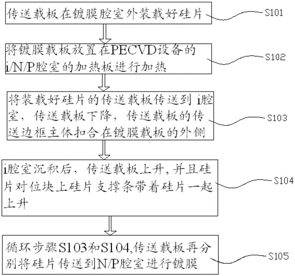
[0032] Such as image 3 As shown, the present invention discloses a method for coating a solar cell, the method includes the following steps:

[0033] S101: The transfer carrier is loaded with silicon wafers outside the coating chamber;

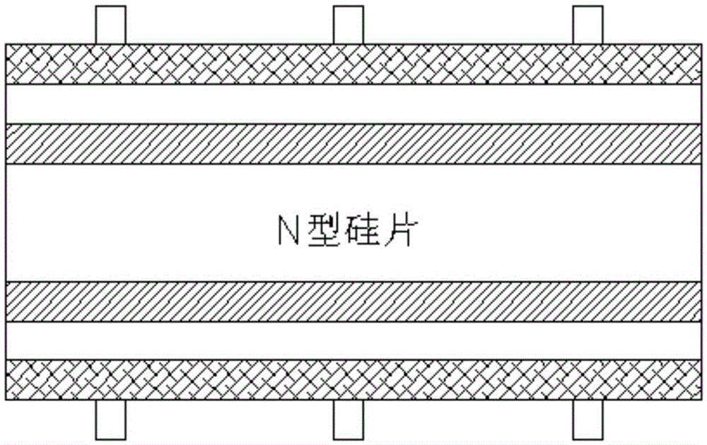
[0034] S102: Place the coating carrier board on the heating plate of the i / N / P chamber of the PECVD equipment for heating;

[0035] S103: The transfer carrier board loaded with silicon wafers is transferred to the i chamber, the transfer carrier board is lowered, and the main body of the transfer frame of the transfer carrier board is buckled on the outside of th...


PUM

PropertyMeasurementUnit
thicknessaaaaaaaaaa
widthaaaaaaaaaa
diameteraaaaaaaaaa

Abstract

The invention discloses a film plating method for a solar cell and support plates. The film plating method comprises the steps that the transmission support plate is loaded with a silicon slice outside a film plating chamber; the film plating support plate is placed on a heating plate of an i/N/P chamber of PECVD equipment to be heated, the film plating support plate comprises a base plate, and the base plate is provided with a silicon slice alignment groove corresponding to a bearing area of the transmission support plate and further provided with a metal wire alignment groove corresponding to a metal wire of the transmission support plate, and a silicon slice alignment block alignment groove corresponding to a silicon slice alignment block of the transmission support plate; the transmission support plate loaded with the silicon slice is transmitted to an i chamber, the transmission support plate declines, the silicon slice on the transmission support plate, the metal wire, the silicon slice alignment block and a silicon slice supporting strip sink into the corresponding alignment grooves in the film plating support plate separately, and a main transmission frame body of the transmission support plate is buckled on the outer side of the film plating support plate; after deposition in the i chamber is completed, the transmission support plate ascends, the silicon slice supporting strip on the silicon slice alignment block carries the silicon slice to rise together; and then, the silicon slice is transmitted to an N/P chamber for film plating through the transmission support plate.

Description

Technical field [0001] The invention relates to the field of solar cells, in particular to a method for coating a solar cell and a carrier board. Background technique [0002] Crystalline silicon solar cells have the advantages of high photoelectric conversion efficiency and mature production technology. They have always accounted for most of the total output of solar cells in the world. However, the high temperature diffusion PN junction process in the production of traditional crystalline silicon solar cells has caused a series of problems And the lack of a good surface passivation mechanism has not been well improved, thus limiting the improvement of battery efficiency. [0003] The solar cell combines the advantages of monocrystalline silicon solar cells and amorphous silicon solar cells. The cell has the characteristics of low temperature in the preparation process, high conversion efficiency, and good high-temperature characteristics. It is a low-cost and high-efficiency cell...

Claims


Application Information

Patent Timeline
Patent Type & Authority Applications(China)
IPC IPC(8): C23C16/458C23C16/513H01L31/18
CPCC23C16/4581C23C16/513H01L31/1868H01L31/1876Y02E10/50Y02P70/50
Inventor 杨与胜王树林宋广华罗骞张超华庄辉虎
Owner GS SOLAR CHINA COMPANY
Why Eureka
Try Eureka