Heterogeneous junction solar cell edge insulating method

A solar cell and edge insulation technology, applied in the field of solar cells, can solve problems such as winding and plating, and achieve the effect of increasing light absorption area, improving production efficiency and conversion efficiency

Inactive Publication Date: 2017-06-09
GS SOLAR CHINA COMPANY
View PDF3 Cites 7 Cited by
  • Summary
  • Abstract
  • Description
  • Claims
  • Application Information

AI Technical Summary

Problems solved by technology

[0005] In view of the above problems, the present invention provides a method for insulating the edges of heterojunction solar cells, which solves the phenomenon of wrapping around when depositing conductive films by sputtering

Method used


Image

  • Heterogeneous junction solar cell edge insulating method
  • Heterogeneous junction solar cell edge insulating method
  • Heterogeneous junction solar cell edge insulating method

Examples


Embodiment

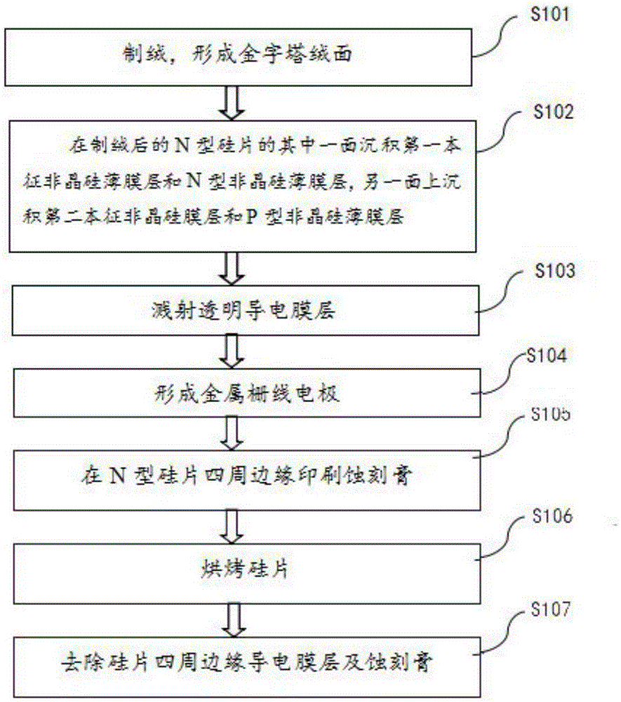
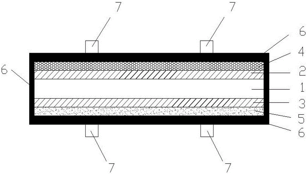
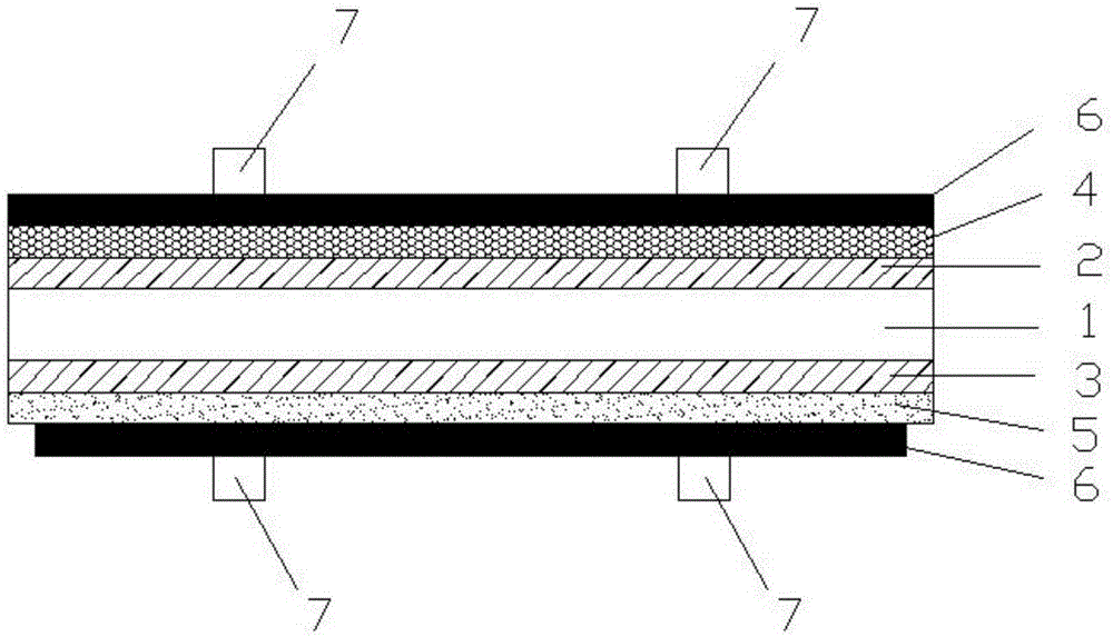
[0023] like Figure 1-3 As shown, the invention discloses a heterojunction solar cell edge insulation method, which includes the following steps:

[0024] S101 Texture cleaning on both sides of the N-type silicon wafer 1 to form a pyramid texture;

[0025] S102 Deposit the first intrinsic layer 2 and the N-type amorphous silicon film layer 4 on one side of the N-type silicon wafer 1 after texturing, and deposit the second intrinsic amorphous silicon film layer 3 and the P-type amorphous silicon film layer 4 on the other side. Silicon film layer 5;

[0026] S103 sputtering the conductive film layer 6 on both sides of the N-type silicon wafer 1;

[0027] S104 forming a metal grid line electrode 7 on the conductive film layer 6 on both sides of the N-type silicon wafer;

[0028] S105 prints etching paste on the surrounding edges of the backlight surface P side or the light receiving surface N surface of the N-type silicon wafer; in an embodiment, the etching paste can be print...


PUM


Abstract

The present invention discloses a heterogeneous junction solar cell edge insulating method. The method includes the following steps that: texturization is performed on two surfaces of an N type silicon wafer, so that pyramid texturized surfaces can be formed; a first intrinsic layer and an N type amorphous silicon thin film layer are deposited on one surface of the texturized N type silicon wafer, a second intrinsic layer and a P type amorphous silicon thin film layer are deposited on the other surface; conductive film layers are formed on the N type amorphous silicon thin film layer and the P type amorphous silicon thin film layer through sputtering; metal grid line electrodes are formed on the conductive film layers; etching paste is printed on the periphery of the shady surface (P surface) or light receiving surface (N surface) of the N type silicon wafer; and the N type silicon wafer printed with the etching paste is baked, and the conductive film layers and the etching paste at the periphery of the wafer can be removed. According to the heterogeneous junction solar cell edge insulating method of the invention adopted, the etching paste is printed at the periphery of the wafer, so that a frame pressing mode conducted in the sputtering process of the conductive thin films can be omitted, and therefore, frame pressing is not required in the deposition process of the conductive thin films, the conductive film layers can be formed on the whole two surfaces of the silicon wafer through sputtering, and the large-scale automated production of the conductive film layers can be benefitted.

Description

technical field [0001] The invention relates to the technical field of solar cells, in particular to an edge insulation method for heterojunction solar cells. Background technique [0002] A solar cell is a semiconductor device that can convert solar energy into electrical energy. Under the condition of light, a photogenerated current will be generated inside the solar cell, and the electrical energy will be output through the electrodes. In recent years, the production technology of solar cells has been continuously improved, the production cost has been continuously reduced, and the conversion efficiency has been continuously improved. The application of photovoltaic power generation has become increasingly widespread and has become an important energy source for power supply. Among them, heterojunction solar cells are a new type of high-efficiency battery technology. [0003] Because heterojunction solar cells are prone to wrapping when sputtering and depositing conductiv...

Claims


Application Information

Patent Timeline
Patent Type & Authority Applications(China)
IPC IPC(8): H01L31/18
CPCH01L31/1804Y02E10/547Y02P70/50
Inventor 黄巍辉张超华罗骞宋广华庄辉虎
Owner GS SOLAR CHINA COMPANY
Why Eureka
Try Eureka