Preparation method of solar cell

A solar cell and seed layer technology, applied in circuits, photovoltaic power generation, electrical components, etc., can solve the problems of increasing the production cost of cells, complicating the production process, affecting the performance of components, etc., which is conducive to large-scale automated production, reducing Mechanical damage, beneficial effect on yield

Inactive Publication Date: 2020-10-27
福建钜能电力有限公司
View PDF6 Cites 0 Cited by
  • Summary
  • Abstract
  • Description
  • Claims
  • Application Information

AI Technical Summary

Problems solved by technology

[0002] During the production process of the battery sheet, it is easy to make the P side and the N side of the battery sheet conduction, which makes the battery sheet short circuit, which directly affects the performance of the module.
[0003] In order to avoid the short circuit of the cell caused by winding plating, many companies use protective paint before deposition, press the frame on the edge of the cell during deposition, or print etching paste on the edge of the cell after deposition to insulate, which will complicate the production process and imperceptibly Increase the production cost of the cell, and it is easy to cause defects such as fragments and broken corners

Method used


Image

  • Preparation method of solar cell
  • Preparation method of solar cell
  • Preparation method of solar cell

Examples


Embodiment

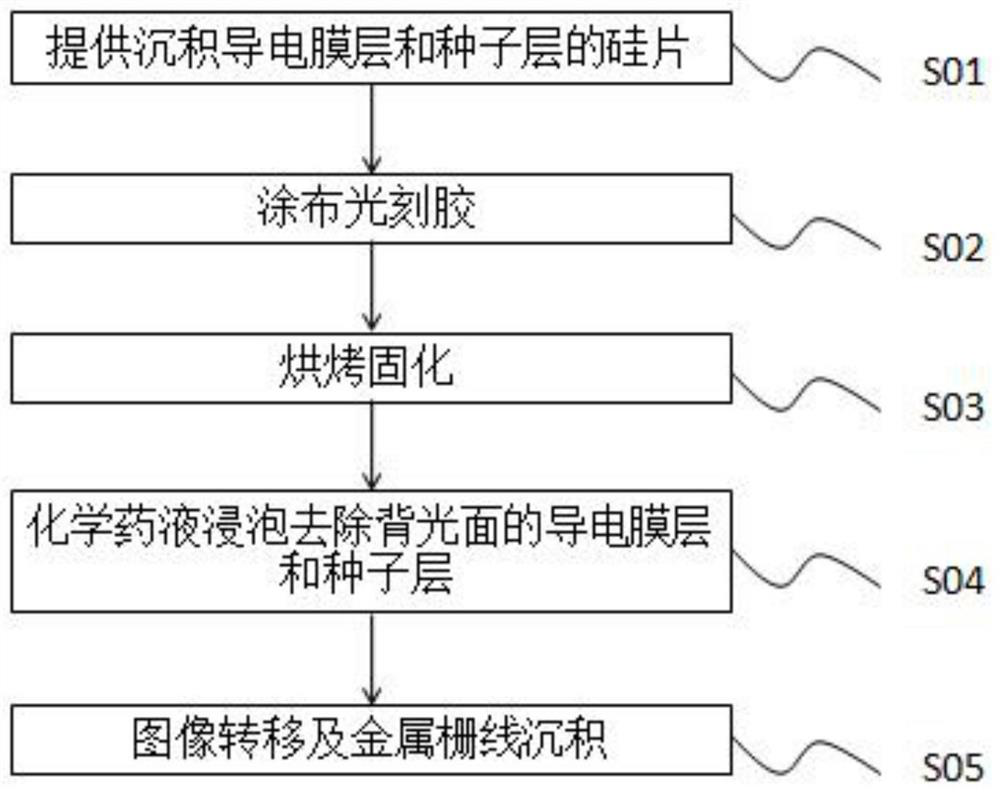
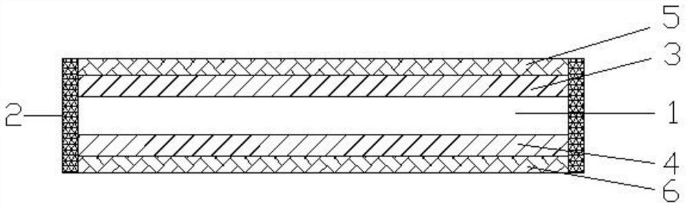
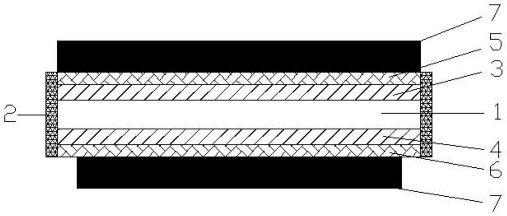
[0029] refer to Figure 1-Figure 5 , a method for preparing a solar cell, comprising the following steps:

[0030] S01, providing a silicon wafer with a conductive film layer and a seed layer deposited on the light incident surface and the backlight surface; when the light incident surface of the silicon wafer 1 is an N-side conductive film layer 3 and a seed layer 5, the backlight surface is P Surface conductive film layer 4, seed layer 6; When the light incident surface is P-side conductive film layer 3, seed layer 5, the backlight surface is N-side conductive film layer 4, seed layer 6. The conductive film layers 3 and 4 are transparent conductive oxide layers TCO with a thickness of 50-200nm; the seed layers 5 and 6 are at least one of Ag, Cu, Al and the like with a thickness of 50-150nm. Such as figure 2 As shown, conductive film layers 3, 4 and seed layers 5, 6 have been deposited on the light incident surface and the backlight surface of the silicon wafer 1, and ther...


PUM

PropertyMeasurementUnit
thicknessaaaaaaaaaa
thicknessaaaaaaaaaa

Abstract

The invention discloses a preparation method of a solar cell. The preparation method comprises the following steps: providing a silicon wafer, wherein a conductive film layer and a seed layer are deposited on the light incident surface and the backlight surface of the silicon wafer; coating the light incident surface and the backlight surface of the silicon wafer respectively with a photoresist; baking and curing the silicon wafer coated with the photoresist; carrying out chemical liquid soaking on the baked and cured silicon wafer; and carrying out pattern transfer and metal electrode deposition on the silicon wafer after insulation processing. According to the invention, a pressing frame is not required to be used in a conductive film deposition process, aand conductive film layers can be sputtered on the whole surfaces of the two surfaces of the silicon wafer, so that a good edge insulation effect can be achieved; a mode of printing etching paste on the edge of a battery sheet is replaced by a mode of soaking and corroding with a chemical solution, so that complete insulation can be realized, the mechanical damage to the battery in the printing process can be reduced, the yieldof a production process and the quality of the battery piece are improved; and the equipment maturity is high, and large-scale automatic production is facilitated.

Description

technical field [0001] The invention relates to the field, in particular to a method for preparing a solar cell. Background technique [0002] During the production process of the battery sheet, it is easy to make the P side of the battery sheet and the N surface of the battery sheet conduct, so that the battery sheet is short-circuited, which directly affects the performance of the module. [0003] In order to avoid the short circuit of the cell caused by winding plating, many companies use protective paint before deposition, press the frame on the edge of the cell during deposition, or print etching paste on the edge of the cell after deposition to insulate, which will complicate the production process and invisibly This increases the production cost of the battery sheet, and is likely to cause defects such as broken pieces and broken corners. Contents of the invention [0004] In view of the above problems, the present invention provides a method for preparing a solar ...

Claims


Application Information

Patent Timeline
Patent Type & Authority Applications(China)
IPC IPC(8): H01L31/18H01L31/0216H01L31/0224H01L21/306
CPCH01L21/30604H01L31/02167H01L31/022425H01L31/1876Y02E10/50
Inventor 宋广华罗骞傅松楠陈伟文
Owner 福建钜能电力有限公司
Why Eureka
Try Eureka