
SiC MOSFET component of slant channel and making method

A technology of devices and slopes, which is applied in the field of SiCMOSFET devices with slope channels and its preparation, can solve problems such as difficult process control, inconsistent crystal surface corrosion rates, and electric field concentration, so as to improve quality, increase channel mobility, and reduce conductivity. The effect of on-resistance

Active Publication Date: 2017-06-13
BEIJING CENTURY GOLDRAY SEMICON CO LTD
View PDF10 Cites 10 Cited by
  • Summary
  • Abstract
  • Description
  • Claims
  • Application Information

AI Technical Summary

Problems solved by technology

The V-shaped groove of the VMOSFET structure is formed by the inconsistent corrosion rate of each crystal plane caused by the anisotropy of SiC under high temperature corrosion, and there is a problem that the process is difficult to control
At the same time, the sharp corners at the bottom of the groove are also likely to cause electric field concentration, resulting in poor reliability

Method used


Image

  • SiC MOSFET component of slant channel and making method
  • SiC MOSFET component of slant channel and making method
  • SiC MOSFET component of slant channel and making method

Examples


Embodiment Construction

[0043] The present invention will now be described more fully with reference to the accompanying drawings, in which exemplary embodiments of the invention are shown. This invention may, however, be embodied in many different forms and should not be construed as limited to the exemplary embodiments set forth herein. Rather, these embodiments are provided so that this disclosure will be thorough and complete, and will fully convey the scope of the invention to those skilled in the art.

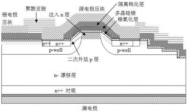
[0044] Such as Figure 4 As shown, the present invention provides a SiC MOSFET device with a slanted channel, and the original cell structure of the active region of the SiC MOSFET device is sequentially drain, n++ substrate, n-drift layer, left and right symmetrically arranged Two p-well layers, p++ area and n++ area arranged on the p-well layer, source electrodes arranged on the p++ area and n++ area; the opposite sides of the two p-well layers are in an upwardly inclined arc shape , above t...


PUM


Abstract

The invention discloses an SiC MOSFET component of a slant channel. A primitive cell structure of an active region of the SiC MOSFET component sequentially comprises a drain electrode, an n++ substrate, an n-drifting layer, two p-well layers arranged in left and right symmetry, a p++ region, an n++ region and a source electrode from bottom to top; the opposite side of the p-well layer is in an arc shape inclined upwards, secondary epitaxy p-type layers which incline toward the vertical central axis of the primitive cell structure are arranged above the arc part of the p-well layer, an injected n layer is arranged between the two secondary epitaxy p-type layers, and an arch-shaped gate oxide layer, an arch-shaped polycrystalline silicone layer and an arch-shaped isolated passivation layer are sequentially arranged above the secondary epitaxy p-type layer and the injected n layer. The invention provides a making method of the SiC MOSFET component of the slant channel. A crystal face with high electron mobility serves as the plane of the channel, the channel is formed in a high-quality secondary-epitaxy SiC surface, the quality of an MOS grating can be effectively improved, the channel mobility can be effectively improved, and on-resistance of the component can be reduced.

Description

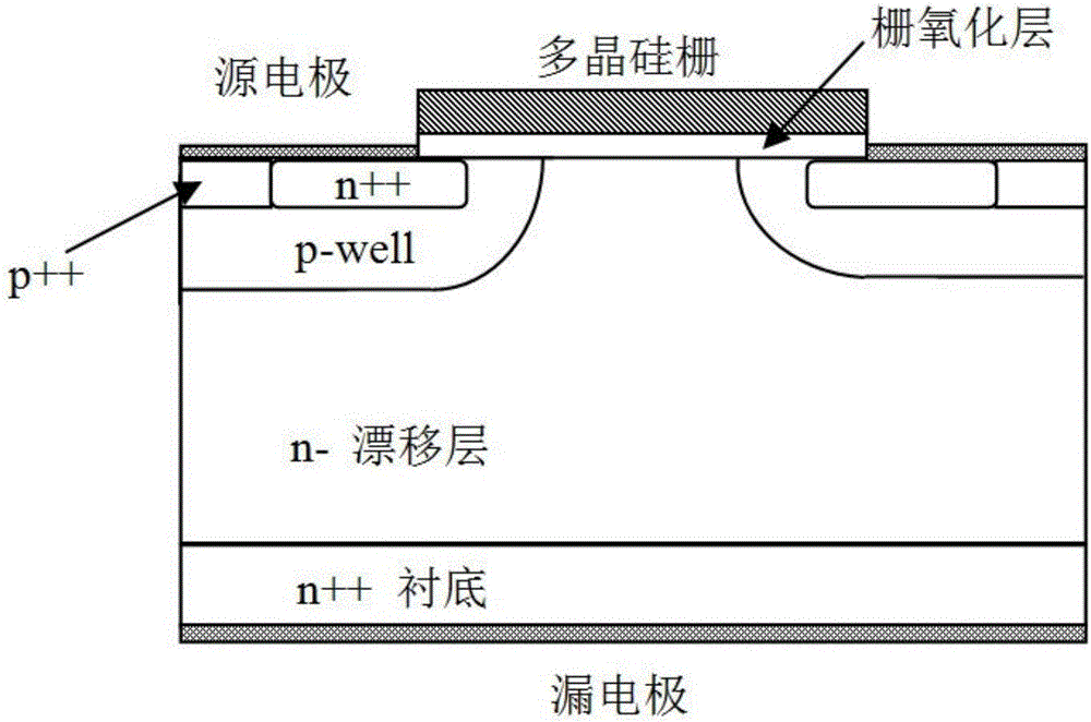
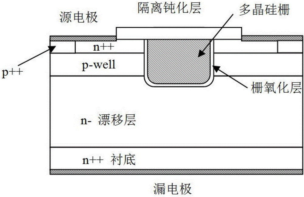
technical field [0001] The invention belongs to the field of semiconductors, and in particular relates to a SiC MOSFET device with a slope channel and a preparation method thereof. Background technique [0002] After years of research in the industry for planar SiC MOSFETs, some manufacturers have taken the lead in launching commercial products. However, there are still problems such as low MOS channel mobility and difficult control of product threshold voltage consistency. This is due to the structure and process of the conventional SiC planar MOSFET. The p-well (p-well) in the conventional MOSFET is doped with p-type by ion implantation. This is a general method in the industry. The structure is as follows: figure 1 shown. This method of high-temperature activation annealing after implantation to form doping inevitably has some problems. The first is that the defects caused by implantation cannot be completely eliminated or repaired, and the second is that the high-temp...

Claims


Application Information

Patent Timeline
Patent Type & Authority Applications(China)
IPC IPC(8): H01L29/06H01L21/336H01L29/78
CPCH01L29/0657H01L29/0661H01L29/66409H01L29/78H01L29/7802H01L29/66068
Inventor 倪炜江
Owner BEIJING CENTURY GOLDRAY SEMICON CO LTD
Learn More