Three-dimensional clock deviation compensation method based on silicon through hole technology and apparatus thereof

A clock deviation and through-silicon via technology is applied in the field of three-dimensional clock deviation compensation based on through-silicon via technology, which can solve problems such as clock deviation and achieve the effect of improving yield

Inactive Publication Date: 2017-06-23
NAT UNIV OF DEFENSE TECH
View PDF2 Cites 6 Cited by
  • Summary
  • Abstract
  • Description
  • Claims
  • Application Information

AI Technical Summary

Problems solved by technology

[0007] The present invention provides a three-dimensional clock offset compensation method and device capable of fast optimization and high-precision fine-tuning of clock path delays, which are used to solve the problem of clock offsets caused by mismatched clock path delays in clock networks of three-dimensional integrated circuits

Method used


Image

  • Three-dimensional clock deviation compensation method based on silicon through hole technology and apparatus thereof
  • Three-dimensional clock deviation compensation method based on silicon through hole technology and apparatus thereof
  • Three-dimensional clock deviation compensation method based on silicon through hole technology and apparatus thereof

Examples


Embodiment Construction

[0053] In order to enable those skilled in the art to better understand the solutions of the present invention, the following will clearly and completely describe the technical solutions in the embodiments of the present invention in conjunction with the drawings in the embodiments of the present invention. Obviously, the described embodiments are only It is an embodiment of a part of the present invention, but not all embodiments. Based on the embodiments of the present invention, all other embodiments obtained by persons of ordinary skill in the art without making creative efforts shall fall within the protection scope of the present invention.

[0054] The method and device for three-dimensional clock offset compensation based on TSV technology provided by the present invention will be further described below with reference to the accompanying drawings.

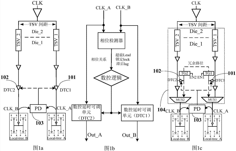
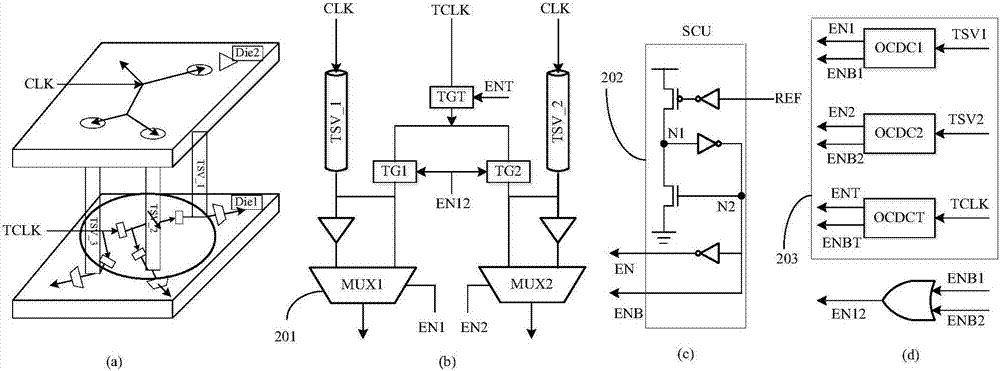
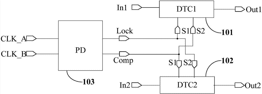
[0055] The invention provides a high-precision three-dimensional clock deviation compensation device. The device mainly...


PUM


Abstract

The invention provides a three-dimensional clock deviation compensation method which can be used to rapidly optimize and carry out high precision fine tuning on clock path delay and an apparatus thereof. The apparatus mainly comprises a phase detector and a numerical control time-delay adjustable unit. The method is used to mainly carry out clock deviation compensation on two three-dimensional clock paths whose delay is not matched in a three-dimensional integrated circuit chip. In the invention, a three-dimensional clock path deviation problem without considering clock TSV fault tolerance can be solved and a clock deviation problem generated because three-dimensional clock path delay is not matched after the clock TSV fault tolerance is considered can be solved too. The method and the apparatus are used to solve the clock deviation problem generated because the clock path delay is not matched in a three-dimensional integrated circuit clock network, which is good for ensuring high reliability of a three-dimensional clock network and increasing a yield of the three-dimensional integrated circuit chip.

Description

technical field [0001] The invention relates to the field of three-dimensional integrated circuit design, in particular to a method and device for compensating three-dimensional clock deviation based on silicon via technology. Background technique [0002] With the increase in integration and performance improvement brought about by the reduction of device size, the semiconductor industry has been following Moore's law for more than half a century. However, as IC technology enters the nanometer era, interconnect propagation delay has replaced gate delay and has become a key factor in determining IC performance and power consumption. That is, it has become the most important bottleneck restricting circuit performance. [0003] The design of three-dimensional integrated circuit chips is generally considered to be one of the most promising technologies to continue and surpass Moore's Law because it overcomes the bottleneck of two-dimensional integrated circuit chip design unde...

Claims


Application Information

Patent Timeline
Patent Type & Authority Applications(China)
IPC IPC(8): H03K5/156
Inventor 赵振宇袁强冯超超徐实马卓马驰远余金山乐大珩何小威王耀刘海斌
Owner NAT UNIV OF DEFENSE TECH
Why Eureka
Try Eureka