Chip protection ring, semiconductor chip, semiconductor wafer and packaging method

A technology for chip packaging and guard rings, applied in semiconductor devices, semiconductor/solid-state device manufacturing, semiconductor/solid-state device components, etc., can solve problems such as chip 10 failure, solder balls are too large, and cannot be re-bonded

Active Publication Date: 2017-06-27
SEMICON MFG INT (SHANGHAI) CORP +1
View PDF3 Cites 17 Cited by
  • Summary
  • Abstract
  • Description
  • Claims
  • Application Information

AI Technical Summary

Problems solved by technology

The inventor found that since the bonding wire 14 is very close to the surface of the chip 10, and the guard ring 12 is also very close to the bonding pad 13, during the bonding process, the solder balls may be too large and shift due to factors such as unstable process conditions. , so it is easy for the welding wire 14 to come into contact with the guard ring 12, causing the protective layer 125 above the guard ring to be crushed, and the welding wire 14 directly contacts the top metal layer 1233 of the guard ring 12 and the topmost metal ring 1231
If a similar situation occurs with other bonding wires, then the two bonding wires 14 are short-circuited due to simultaneous contact with the top metal layer 12313 of the top metal layer of the guard ring 12, which is very likely to cause the chip 10 to fail, such as some functions of the chip 10 Does not work properly or the performance of the chip does not meet the design requirements
And remanufacturing wafers with the same process conditions will cost a lot of manpower and financial resources
If the solder balls are corroded by acid solution, the aluminum on pad 13 will also be corroded and cannot be re-bonded

Method used


Image

  • Chip protection ring, semiconductor chip, semiconductor wafer and packaging method
  • Chip protection ring, semiconductor chip, semiconductor wafer and packaging method
  • Chip protection ring, semiconductor chip, semiconductor wafer and packaging method

Examples


Embodiment Construction

[0046]In order to make the purpose and features of the present invention more obvious and understandable, the specific implementation of the present invention will be further described below in conjunction with the accompanying drawings. However, the present invention can be implemented in different forms and should not be limited to the described embodiments.

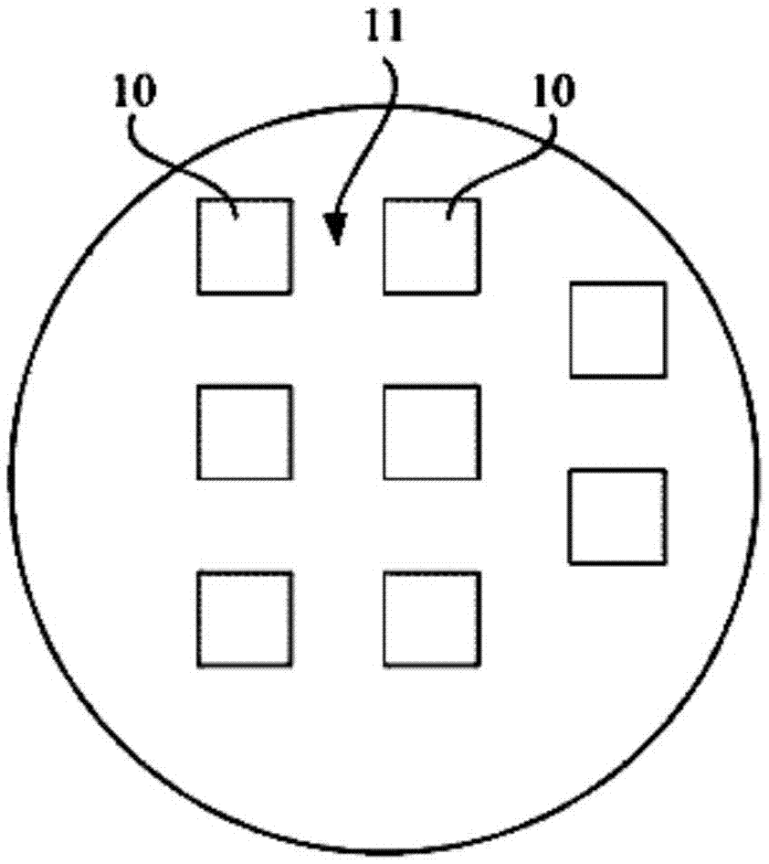
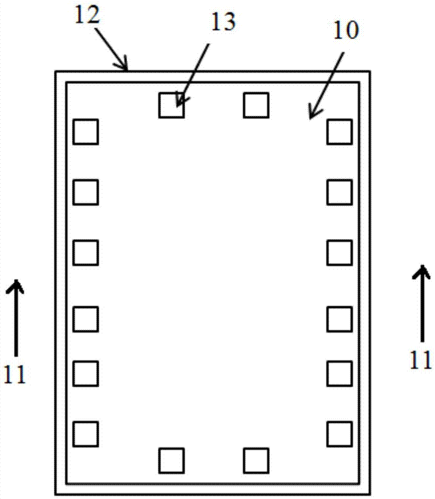
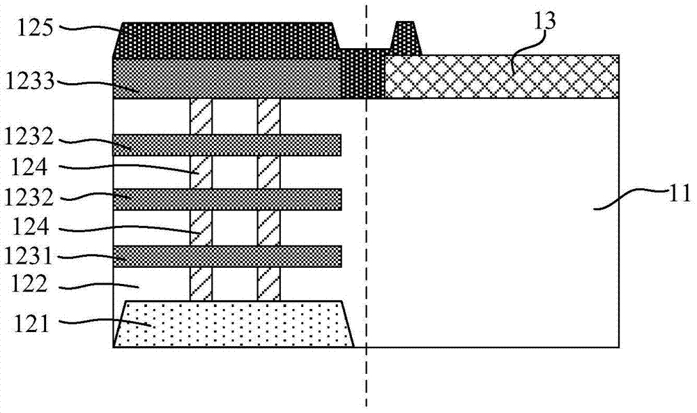
[0047] Please also refer to Figures 5A to 5D , the present invention proposes a chip protection ring (seal ring) 12, arranged around a chip and formed on the same semiconductor substrate (not shown) with the chip, the chip protection ring 12 includes a seal ring supported by the semiconductor substrate Several metal rings 123 stacked in sequence and conductive plugs 124 arranged between adjacent metal rings, and each metal ring 123 is arranged around the chip, wherein the top metal ring (top metal, TM) 1231 is Discontinuous metal rings are disconnected between adjacent bonding pads (Pad) 13 of the chip, the radius of ...


PUM


Abstract

The invention provides a chip protection ring, a semiconductor chip, a semiconductor wafer and a packaging method. Through breaking a metal ring in the topmost layer of the protection ring near each bonding pad and reducing the size of a metal ring in the second topmost layer, a conductive plug in the topmost layer is not contacted with the metal ring in the second topmost layer and the rest below metal rings, the metal ring in the topmost layer is thus isolated and suspended, short circuit does not happen to bonding wires even if the bonding wires are contacted with the metal ring in the topmost layer in the case of packaging and bonding, and while short circuit between the bonding wires can be prevented, a protection role of the protection ring can still be ensured.

Description

technical field [0001] The invention relates to the technical field of semiconductor manufacturing, in particular to a chip protection ring, a semiconductor chip, a semiconductor wafer and a packaging method. Background technique [0002] In the semiconductor manufacturing process, usually, the wafer formed with the integrated circuit is cut into individual chips (chips), and then these chips are manufactured into semiconductor package structures with different functions. Specific reference figure 1 , figure 1 It is a top view of the wafer, and the wafer is composed of a plurality of chips 10 , and two adjacent chips 10 are separated by scribe lines (or scribe lines, or blocks) 11 . Each chip 10 includes a device structure, an interconnection structure, and pads formed on a substrate through processes such as deposition, photolithography (lithography), etching, doping, and heat treatment. Afterwards, the wafer is diced into a plurality of independent chips 10 along the di...

Claims


Application Information

Patent Timeline
Patent Type & Authority Applications(China)
IPC IPC(8): H01L23/04H01L21/56
CPCH01L21/56H01L23/04H01L2224/05H01L2224/05554H01L2224/49175
Inventor 何明
Owner SEMICON MFG INT (SHANGHAI) CORP
Why Eureka
Try Eureka