Liquid crystal display panel and manufacturing method thereof as well as array substrate

A technology for liquid crystal display panels and array substrates, applied in nonlinear optics, instruments, optics, etc., can solve the problems of reducing the light transmittance of liquid crystal display panels 10, high manufacturing costs, etc.

Active Publication Date: 2017-06-30
WUHAN CHINA STAR OPTOELECTRONICS TECH CO LTD
View PDF7 Cites 8 Cited by
  • Summary
  • Abstract
  • Description
  • Claims
  • Application Information

AI Technical Summary

Problems solved by technology

These layer structures generally require 9-14 processes, which not only makes the manufacturing cost high, but also reduces the light transmittance of the liquid crystal display panel 10 in each process.

Method used


Image

  • Liquid crystal display panel and manufacturing method thereof as well as array substrate
  • Liquid crystal display panel and manufacturing method thereof as well as array substrate
  • Liquid crystal display panel and manufacturing method thereof as well as array substrate

Examples


Embodiment Construction

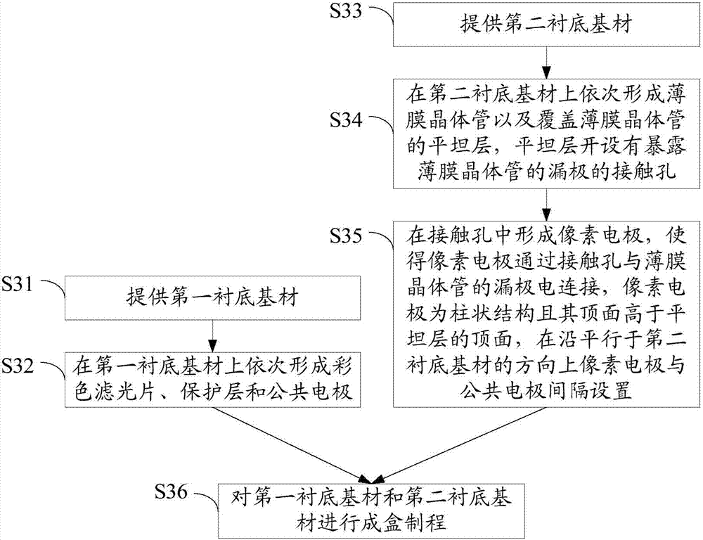
[0013] The technical solutions of each exemplary embodiment provided by the present invention will be described clearly and completely in conjunction with the accompanying drawings in the embodiments of the present invention. In the case of no conflict, the following embodiments and features in the embodiments can be combined with each other.

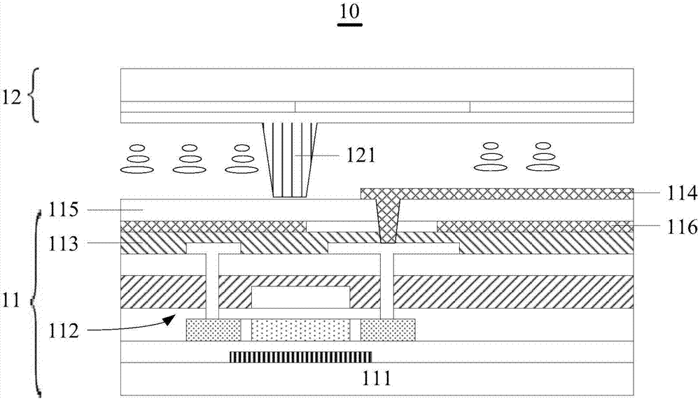
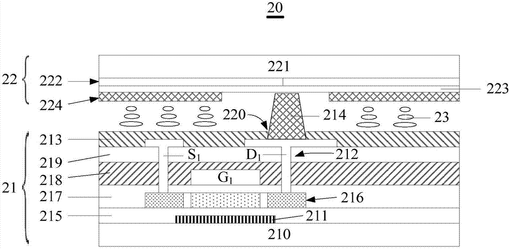
[0014] See figure 2 , Is the liquid crystal display panel of the first embodiment of the present invention. The liquid crystal display panel 20 includes a relatively spaced array substrate (Thin Film Transistor Substrate, referred to as TFT substrate, also referred to as thin film transistor substrate or Array substrate) 21 and a color filter substrate (Color Filter Substrate, referred to as CF substrate, also referred to as color filter substrate). Sheet substrate) 22 and liquid crystal (liquid crystal molecules) 23 filled between the two substrates. The liquid crystal 23 is located in a liquid crystal cell formed by superimposing and s...


PUM


Abstract

The invention discloses a liquid crystal display panel and a manufacturing method thereof as well as an array substrate. Common electrodes are arranged at one side of a color film substrate; pixel electrodes are formed in contact holes in a flat layer of the array substrate and are electrically connected with a drain of a thin-film transistor through the contact holes; the pixel electrodes are of a columnar structure and the top surfaces of the pixel electrodes are higher than that of the flat layer; and the pixel electrodes and the common electrodes are arranged at an interval along the direction parallel to the array substrate. Therefore, the manufacture procedure of the liquid crystal display panel can be simplified, the light transmissivity is improved and the influence of an electric field between the adjacent pixel electrodes is reduced.

Description

Technical field [0001] The present invention relates to the field of liquid crystal display technology, in particular to a liquid crystal display panel, a manufacturing method thereof, and an array substrate. Background technique [0002] LTPS (Low Temperature Poly-silicon, low temperature polysilicon technology) liquid crystal display panels have come to the fore in the display field due to their high electron mobility and high brightness. However, its structure has many layers and the manufacturing process is more complicated. Such as figure 1 As shown, in the structure design of the existing LTPS liquid crystal display panel 10, the color filter substrate 12 is provided with a PS (Photo Space, spacer) 121 on the side facing the array substrate 11. The array substrate 11 includes a substrate substrate 111 and Each layer structure on the substrate 111, such as a thin film transistor 112, a planarization layer (PLN) 113, a pixel electrode 114, a passivation layer (abbreviation) ...

Claims


Application Information

Patent Timeline
Patent Type & Authority Applications(China)
IPC IPC(8): G02F1/1343G02F1/1362
CPCG02F1/134309G02F1/136227
Inventor 李安石
Owner WUHAN CHINA STAR OPTOELECTRONICS TECH CO LTD
Why Eureka
Try Eureka