

PCB surface automatic film plating process
A PCB board, automatic technology, applied in the field of automatic coating process on the surface of PCB board, can solve problems such as insufficient, PCB color difference, film thickness, etc., to achieve the effect of uniform erosion, uniform thickness, and enhanced cleaning effect
- Summary
- Abstract
- Description
- Claims
- Application Information
AI Technical Summary
Problems solved by technology
Method used
Image

Examples
Embodiment 1
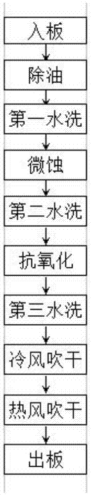
[0020] Such as figure 1 An automatic coating process on the surface of a PCB board as shown, comprising the following steps:
[0021] 1) Board entry: Manually place the PCB board on the transfer roller of the entry station of the automatic anti-oxidation machine production line;
[0022] 2) Degreasing: The PCB board passes through the degreasing station evenly with the conveying roller, and the nozzle installed at the degreasing station sprays the degreasing agent to the surface of the PCB board;
[0023] 3) The first water washing: the PCB board prepared in step 2) is transported to the first water washing station through the transfer roller and cleaned with a water knife. The number of the first water washing stations is 3, and the pressure of the water knife is For: 2kg / cm 2 ;
[0024] 4) Micro-etching: The PCB board prepared in step 3) is transported to the micro-etching station by the transfer roller and immersed in the micro-etching tank for anti-oxidation treatment, ...
Embodiment 2
[0033] An automatic coating process on the surface of a PCB, comprising the following steps:
[0034] 1) Board entry: Manually place the PCB board on the transfer roller of the entry station of the automatic anti-oxidation machine production line;
[0035] 2) Degreasing: The PCB board passes through the degreasing station evenly with the conveying roller, and the nozzle installed at the degreasing station sprays the degreasing agent to the surface of the PCB board;
[0036] 3) The first water washing: the PCB board prepared in step 2) is transported to the first water washing station through the transfer roller and cleaned with a water knife. The number of the first water washing stations is 3, and the pressure of the water knife is For: 2.2kg / cm 2 ;
[0037] 4) Micro-etching: The PCB board prepared in step 3) is transported to the micro-etching station by the transfer roller and immersed in the micro-etching tank for anti-oxidation treatment, and the micro-etching solution ...
Embodiment 3
[0046] An automatic coating process on the surface of a PCB, comprising the following steps:
[0047] 1) Board entry: Manually place the PCB board on the transfer roller of the entry station of the automatic anti-oxidation machine production line;
[0048] 2) Degreasing: The PCB board passes through the degreasing station evenly with the conveying roller, and the nozzle installed at the degreasing station sprays the degreasing agent to the surface of the PCB board;
[0049]3) The first water washing: the PCB board prepared in step 2) is transported to the first water washing station through the transfer roller and cleaned with a water knife. The number of the first water washing stations is 3, and the pressure of the water knife is For: 2.1kg / cm 2 ;
[0050] 4) Micro-etching: The PCB board prepared in step 3) is transported to the micro-etching station by the transfer roller and immersed in the micro-etching tank for anti-oxidation treatment, and the micro-etching solution i...
PUM
 Abstract
Description
Claims
Application Information