High-electron-mobility transistor and memory chip

A high electron mobility, transistor technology, used in semiconductor devices, semiconductor/solid-state device manufacturing, circuits, etc., can solve problems such as low heat, lower on-resistance, and difficulty in obtaining devices

Inactive Publication Date: 2017-07-07
PEKING UNIV +2
View PDF4 Cites 2 Cited by
  • Summary
  • Abstract
  • Description
  • Claims
  • Application Information

AI Technical Summary

Problems solved by technology

[0005] However, the use of GaN materials and non-doped intrinsic materials makes it difficult to obtain HEMT (High Electron Mobility Transistor, High Electron Mobility Transistor) devices with low on-resistance, and for high-power high-frequency devices, low conduction On-resistance often means low heat generation and high reliability performance, so reducing the on-resistance value is one of the key technologies for HEMT manufacturing

Method used


Image

  • High-electron-mobility transistor and memory chip
  • High-electron-mobility transistor and memory chip

Examples


Embodiment Construction

[0028] In order to understand the above-mentioned purpose, features and advantages of the present invention more clearly, the present invention will be further described in detail below in conjunction with the accompanying drawings and specific embodiments. It should be noted that, in the case of no conflict, the embodiments of the present application and the features in the embodiments can be combined with each other.

[0029] In the following description, many specific details are set forth in order to fully understand the present invention. However, the present invention can also be implemented in other ways different from those described here. Therefore, the protection scope of the present invention is not limited by the specific details disclosed below. EXAMPLE LIMITATIONS.

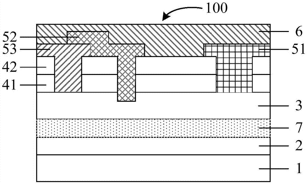
[0030] figure 1 A schematic structural diagram of a high electron mobility transistor according to an embodiment of the present invention is shown.

[0031] like figure 1 As shown, the high electr...


PUM


Abstract

The invention provides a high-electron-mobility transistor and a memory chip. The high-electron-mobility transistor comprises a substrate, a gallium nitride layer, a gallium nitride aluminum layer, an insulating layer and an electrode, wherein one side of the gallium nitride layer is compounded on a surface layer of the substrate and the other side of the gallium nitride layer is compounded on a bottom portion of the gallium nitride aluminum layer; the insulating layer is compounded on a top layer of the gallium nitride aluminum layer, and the insulating layer is provided with at least three cut-through contact holes; and the electrode includes a drain electrode, a gate electrode and a source electrode, and the drain electrode, the gate electrode and the source electrode are arranged in the corresponding contact holes of the at least three corresponding cut-through contact holes, the gate electrode is extended to the source electrode from a pole plate outside the contact holes so as to realize contact of the gate electrode and the source electrode. In the technical scheme, a space between the gate electrode and the source electrode is eliminated, a conduction resistance and power consumption of the high-electron-mobility transistor are effectively reduced and reliability of the high-electron-mobility transistor is increased.

Description

technical field [0001] The invention relates to the technical field of semiconductors, in particular to a high electron mobility transistor and a memory chip. Background technique [0002] In related technologies, with the development of semiconductor manufacturing technology, power devices with low power consumption and high-speed high-pass characteristics have become the mainstream research direction. [0003] GaN (Gallium Nitride) is the third generation wide bandgap semiconductor material with large bandgap (3.4eV), high electron saturation rate (2e7cm / s), high breakdown electric field (1e10--3e10V / cm), relatively It has high thermal conductivity, corrosion resistance and radiation resistance, and has strong advantages in high pressure, high frequency, high temperature, high power and radiation resistance environmental conditions, so it is considered to be a research tool for short-wave optoelectronic devices and high-voltage, high-frequency and large Optimal material f...

Claims


Application Information

Patent Timeline
IPC IPC(8): H01L29/778H01L29/41H01L21/335
Inventor 刘美华陈建国林信南
Owner PEKING UNIV
Why Eureka
Try Eureka