Wiring structure, display substrate and display device
A technology for display substrates and line structures, which is applied in identification devices, nonlinear optics, instruments, etc., can solve problems such as metal trace breakage and display device failure, and achieve the effect of improving yield and ensuring yield.
- Summary
- Abstract
- Description
- Claims
- Application Information
AI Technical Summary
Problems solved by technology
Method used
Image

Examples
Embodiment 1
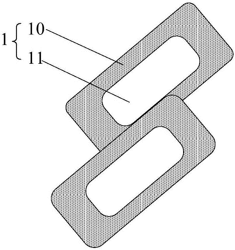
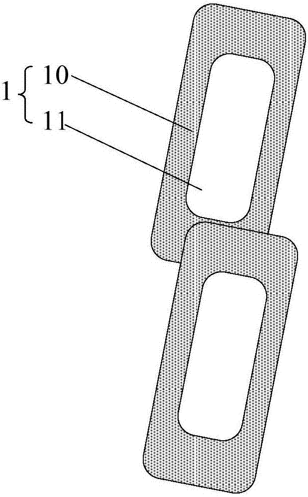
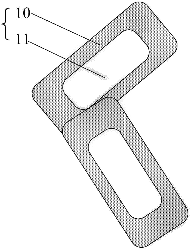
[0022] combine Figure 1-4 As shown, this embodiment provides a wiring structure, which includes a plurality of hollowed-out units 1 connected in series, and each hollowed-out unit 1 includes a hollowed-out area 11 and a non-hollowed-out area 10; wherein, any two adjacent The hollowed-out areas 11 of the hollowed-out unit 1 at least partially overlap, and the non-hollowed-out areas 10 do not overlap.
[0023] It should be noted here that the positions where the hollowed out regions 11 of any two adjacent hollowed out units 1 at least partially overlap may be structures formed on the same layer during manufacture, that is, the two hollowed out units 1 are in the same layer. Of course, the two hollow units 1 can also be arranged in two layers. In this case, an insulating layer needs to be arranged between the layers of the two hollow units 1 during preparation, and then the insulating layer and the two A via hole is formed at the connected position so that the two can be electr...
Embodiment 2
[0035] This embodiment provides a display substrate, which includes a base and a wiring structure disposed on the base, and the wiring structure may be any wiring structure in Embodiment 1.
[0036] The display substrate in this embodiment is preferably a flexible substrate, that is, the material of the substrate used is a flexible material, such as polyimide (PI).
[0037] Since the routing structure in the display substrate in this embodiment includes a plurality of hollowed-out units 1, the routing structure can release stress through the hollowed-out units 1 on the display substrate during bending, stretching, and twisting. In order to avoid breakage, which affects the failure of devices on the substrate to which the wiring structure is applied. Especially for flexible substrates, due to the nature of the flexible substrate itself, it is easy to bend. Adopting the routing structure in this embodiment can greatly improve the yield of the flexible substrate.
Embodiment 3
[0039] This embodiment provides a display device, which includes the display substrate in Embodiment 2. Therefore, the performance of the display device of this embodiment is better.
[0040]Wherein, the display device can be a liquid crystal display device or an electroluminescence display device, such as a liquid crystal panel, an electronic paper, an OLED panel, a mobile phone, a tablet computer, a TV set, a monitor, a notebook computer, a digital photo frame, a navigator, etc. product or part.
PUM
 Abstract
Description
Claims
Application Information
 - R&D
- Intellectual Property
- Life Sciences
- Materials
- Tech Scout
- Unparalleled Data Quality
- Higher Quality Content
- 60% Fewer Hallucinations
Browse by: Latest US Patents, China's latest patents, Technical Efficacy Thesaurus, Application Domain, Technology Topic, Popular Technical Reports.
© 2025 PatSnap. All rights reserved.Legal|Privacy policy|Modern Slavery Act Transparency Statement|Sitemap|About US| Contact US: help@patsnap.com