Thin film transistor, manufacturing method therefor and array substrate

A technology of thin film transistors and manufacturing methods, applied in the direction of transistors, semiconductor/solid-state device manufacturing, semiconductor devices, etc., can solve problems such as weakening, conductive channel corrosion damage, metal surface oxidation, etc., to achieve miniaturization, avoid corrosion damage, The effect of downsizing

Active Publication Date: 2017-07-21
FUZHOU BOE OPTOELECTRONICS TECH CO LTD +1
View PDF4 Cites 5 Cited by
  • Summary
  • Abstract
  • Description
  • Claims
  • Application Information

AI Technical Summary

Problems solved by technology

But, just because the source 6, the drain 7 of the BCE thin film transistor and the active layer 4 are arranged in the same layer, in the process of etching the source 6 and the drain 7, the etching of the source 6 and the drain 7 The conductive channel of the active layer 4 formed before the liquid is easy to corrode and damage; and when the etching of the source electrode 6 and the drain electrode 7 is completed, when the conductive channel of the active layer 4 is subjected to plasma oxidation treatment, the source electrode 6 and the drain electrode The etched metal surface of the drain electrode 7 is also easily oxidized by the plasma oxidation treatment
Therefore, in the manufacturing process of the BCE thin film transistor, it is easy to occur that the conductive channel of the active layer 4 is corroded and damaged, or the source electrode 6 and the drain electrode 7 are oxidized, or the conductive channel of the active layer 4 is corroded and damaged and the source The case where the pole 6 and the drain 7 are oxidized, thereby weakening or damaging the conductivity of the BCE thin film transistor and reducing the yield of the BCE thin film transistor

Method used


Image

  • Thin film transistor, manufacturing method therefor and array substrate
  • Thin film transistor, manufacturing method therefor and array substrate
  • Thin film transistor, manufacturing method therefor and array substrate

Examples


Embodiment Construction

[0037] In order to further illustrate the thin film transistor, its manufacturing method, and array substrate provided by the embodiments of the present invention, a detailed description will be given below in conjunction with the accompanying drawings.

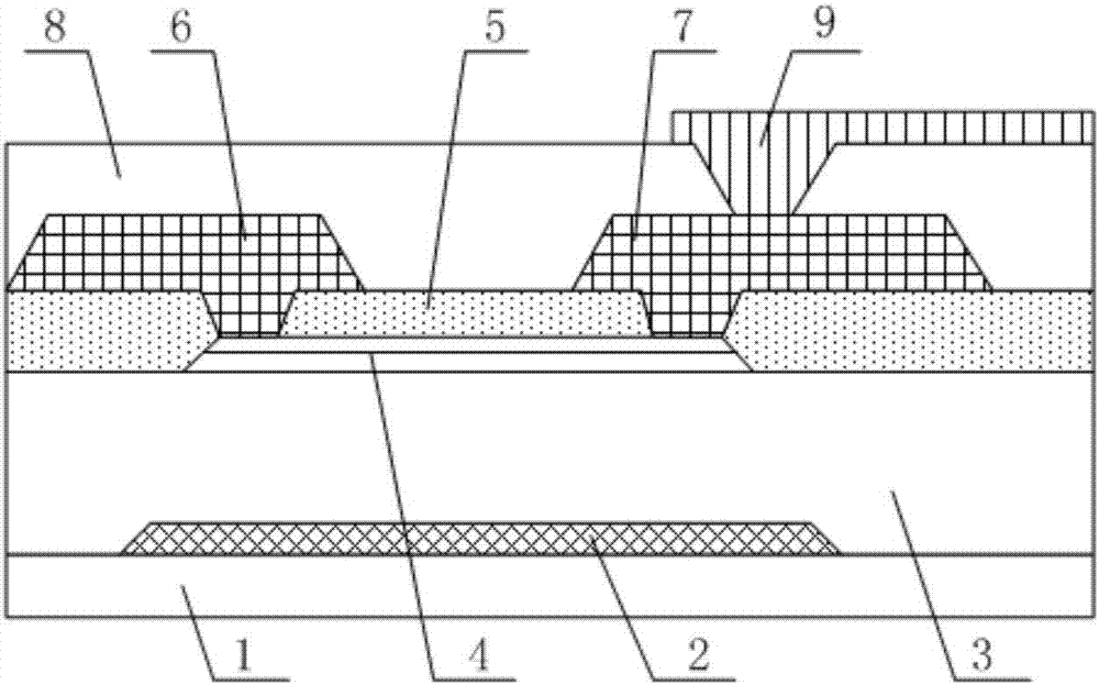
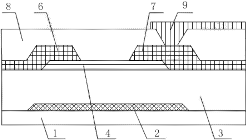
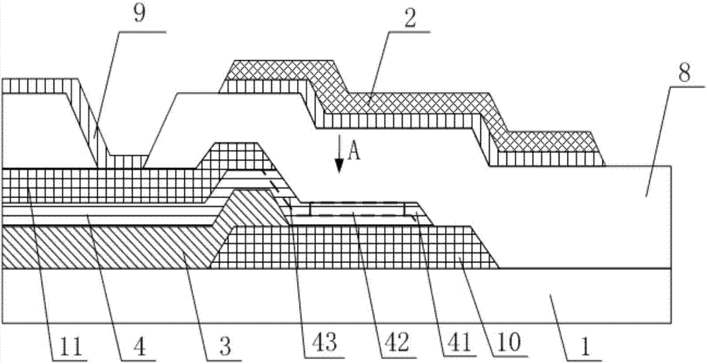
[0038] refer to image 3 and Figure 4 The thin film transistor provided by the embodiment of the present invention is formed on the base substrate 1, and the thin film transistor includes a gate 2 and an active layer 4; the active layer 4 is provided with a first signal metal layer 10 on the surface facing the base substrate 1, and has A second signal metal layer 11 is provided on the surface of the source layer 4 away from the first signal metal layer 10; the active layer 4 includes a conductive channel formation region 42, and the second signal metal layer 11 does not cover the conductive channel formation region of the active layer 4 42.

[0039] During specific implementation, the second signal metal layer 11 and the f...


PUM


Abstract

The invention discloses a thin film transistor, a manufacturing method therefor and an array substrate and relates to the technical field of display technology; the thin film transistor, the manufacturing method therefor and the array substrate are used for improving a yield rate of the thin film transistor while downsizing the thin film transistor. The thin film transistor is formed on a substrate base plate and comprises a grid and an active layer; a surface, facing to substrate base plate, of the active layer is provided with a first signal metal layer; a surface, facing away from the first signal metal layer, of the active layer is provided with a second signal metal layer; the active layer comprises an electric conduction channel forming zone; the second signal metal layer does not cover the electric conduction channel forming zone of the active layer. The thin film transistor, the manufacturing method therefor and the array substrate are used for downsizing the thin film transistor.

Description

technical field [0001] The invention relates to the field of display technology, in particular to a thin film transistor, a manufacturing method thereof, and an array substrate. Background technique [0002] In recent years, with the development of large-scale liquid crystal displays and active organic light-emitting diodes, traditional amorphous silicon thin-film transistors and organic thin-film transistors have been difficult to meet user needs, and Indium Gallium Zinc Oxide (Indium Gallium Zinc Oxide, referred to as The transparent amorphous oxide semiconductor represented by IGZO) has the advantages of high mobility, good uniformity, and transparency, and is widely used in the active layer of the oxide thin film transistor, so that the oxide thin film transistor can meet the requirements of the new generation display. user needs. [0003] At present, the common oxide thin film transistors mainly include the following two types, one is an etching stop layer (hereinafter...

Claims


Application Information

Patent Timeline
Patent Type & Authority Applications(China)
IPC IPC(8): H01L27/12H01L29/786H01L21/77
CPCH01L27/1225H01L27/124H01L27/1259H01L29/7869H01L29/78642H01L29/42384H01L29/78633H01L29/78696H01L27/1262H01L29/41733
Inventor 刘晓伟刘勃黄中浩樊超王洋安亚斌刘正
Owner FUZHOU BOE OPTOELECTRONICS TECH CO LTD
Why Eureka
Try Eureka