

Organic field-effect transistor memory with self-blocking layer structure and fabrication method of organic field-effect transistor memory
An organic field and barrier layer technology, applied in the field of organic field effect transistor memory and its preparation, can solve the problems of not extensive material sources, low data stability, low light response speed, etc., to improve storage performance and photosensitivity performance, high Storage density, the effect of improving storage density
- Summary
- Abstract
- Description
- Claims
- Application Information
AI Technical Summary
Problems solved by technology
Method used
Image

Examples
Embodiment 1
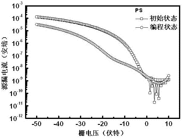
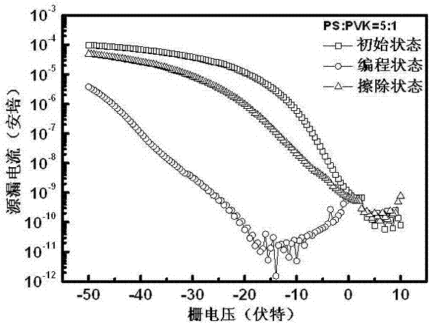
[0034] Such as Figure 1-9 As shown, the first step: at 25°C, prepare polystyrene PS solution with a solution concentration of 5 mg / ml, and let it stand for 12 h in a solution where the solvent is toluene to make it evenly dispersed;
[0035] Step 2: Prepare polyvinylcarbazole PVK solution with a solution concentration of 5 mg / ml, and let it stand in a solution where the solvent is toluene for 2 hours to make it evenly dispersed;
[0036] Step 3: Dope the prepared PS solution and PVK solution according to the volume ratio of 1:1, 5:1, 10:1 and 1:0 respectively;
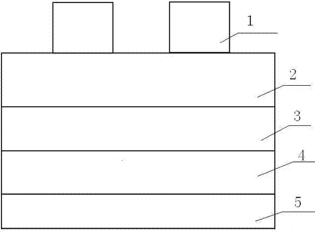
[0037] The fourth step: sequentially form a gate electrode and a gate insulating layer 4 on the substrate 5, the thickness of the gate insulating layer 4 is 300 nm, and make a substrate, and the substrate is ultrasonically cleaned with acetone, ethanol, and deionized water for 10 minutes in sequence, The ultrasonic frequency is 100 KHz, and then the liquid on the surface of the substrate is blown dry with high-purity...
Embodiment 2
[0052] Step 1: Prepare polymethyl methacrylate PMMA solution at 25°C with a solution concentration of 5 mg / ml, and let it stand in a solution with toluene as the solvent for 12 h to make it evenly dispersed;
[0053] Step 2: Prepare polyvinylcarbazole PVK solution with a solution concentration of 5 mg / ml, and let it stand in a solution where the solvent is toluene for 2 hours to make it evenly dispersed;
[0054] The third step: Dope the configured PMMA solution and PVK solution according to the volume ratio of 1:1, 5:1, 10:1 and 1:0 respectively;
[0055] The fourth step: sequentially form a gate electrode and a gate insulating layer 4 on the substrate 5, the thickness of the gate insulating layer 4 is 300 nm, and make a substrate, and the substrate is ultrasonically cleaned with acetone, ethanol, and deionized water for 10 minutes in sequence, The ultrasonic frequency is 100 KHz, and then the liquid on the surface of the substrate is blown dry with high-purity nitrogen to en...
PUM
 Abstract
Description
Claims
Application Information