
CMOS image sensor, and pixel circuit and driving method thereof

An image sensor, pixel circuit technology, applied in circuits, image communication, television, etc., can solve problems such as rising production costs

Active Publication Date: 2017-07-25
BOE TECH GRP CO LTD
View PDF4 Cites 11 Cited by
  • Summary
  • Abstract
  • Description
  • Claims
  • Application Information

AI Technical Summary

Problems solved by technology

In this case, since the working voltage of the integrated circuit (Integrated Circuit, IC) receiving the output signal of the pixel circuit is a positive voltage, in order to match the output voltage of the pixel circuit with the IC, an additional interface circuit needs to be added to the IC , which will lead to an increase in the production cost of the IC

Method used


Image

  • CMOS image sensor, and pixel circuit and driving method thereof
  • CMOS image sensor, and pixel circuit and driving method thereof
  • CMOS image sensor, and pixel circuit and driving method thereof

Examples


Embodiment Construction

[0030] The following will clearly and completely describe the technical solutions in the embodiments of the present invention with reference to the accompanying drawings in the embodiments of the present invention. Obviously, the described embodiments are only some, not all, embodiments of the present invention. Based on the embodiments of the present invention, all other embodiments obtained by persons of ordinary skill in the art without making creative efforts belong to the protection scope of the present invention.

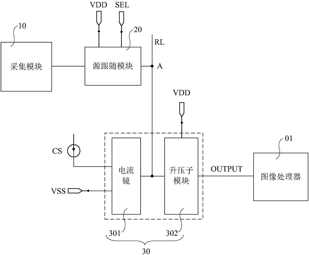
[0031] An embodiment of the present invention provides a pixel circuit of a CMOS image sensor, which is used for figure 1 The image processor 01 shown outputs an acquisition signal. Wherein, the image processor 01 is used to integrate the collected signals of each pixel circuit and output image data.

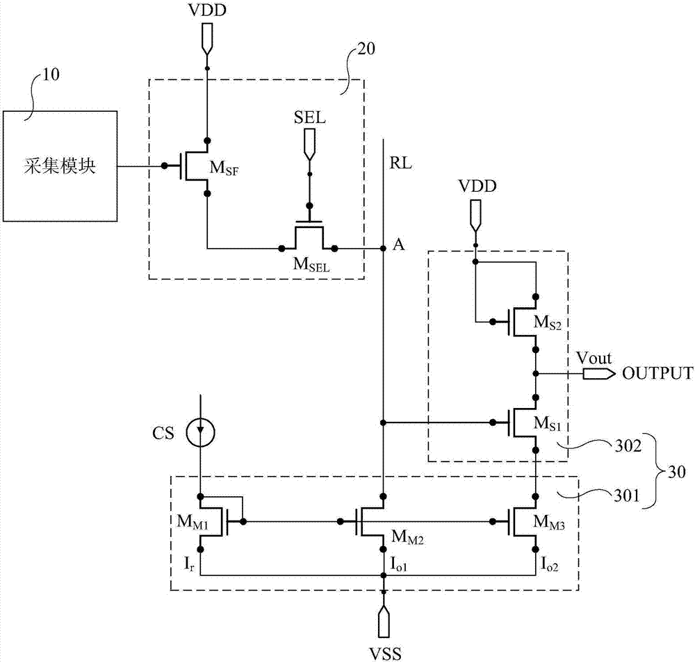
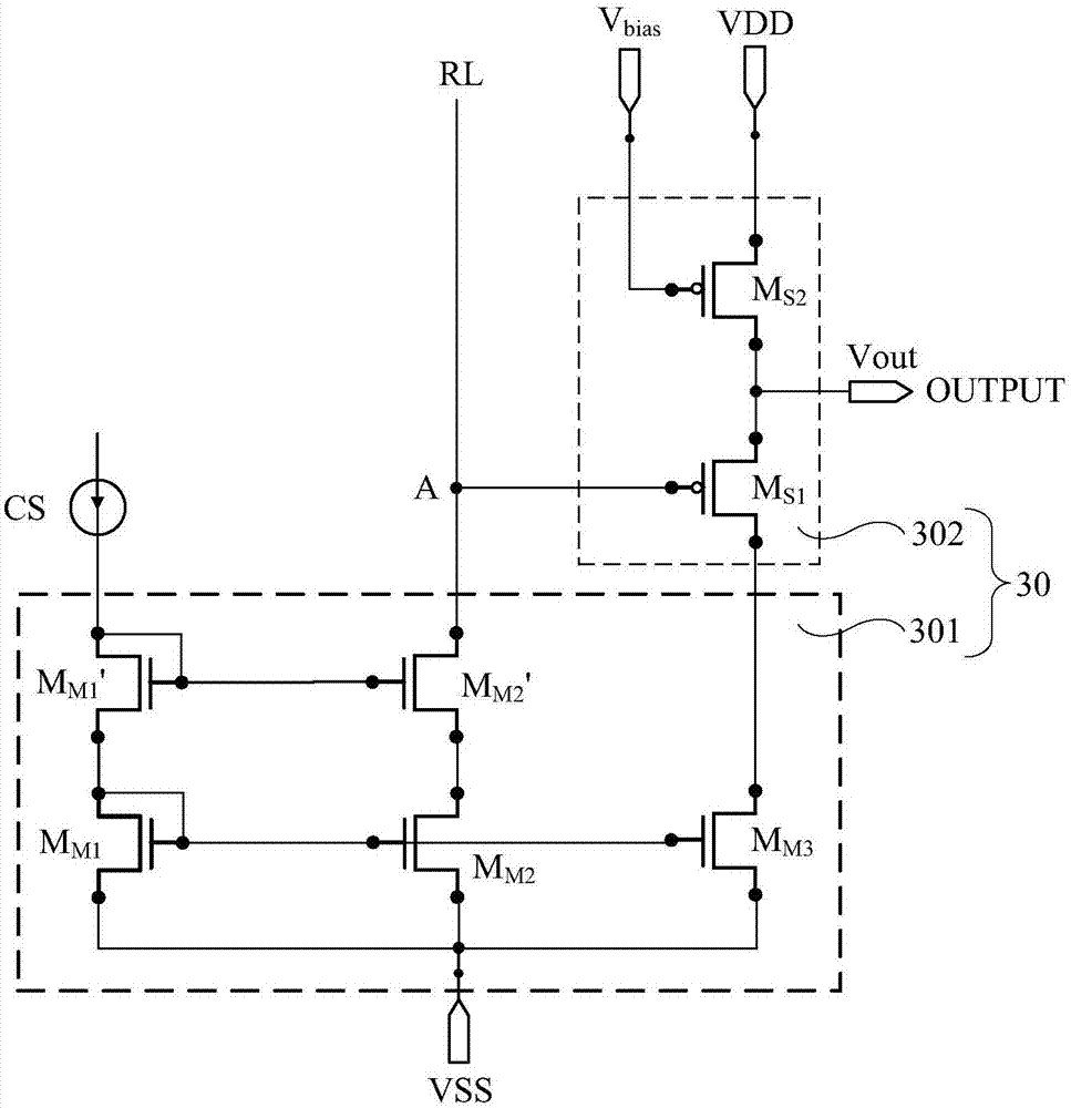
[0032] Based on this, the pixel circuit includes an acquisition module 10 , a source follower module 20 and a voltage conversion module 30 .

[0033] Specific...


PUM


Abstract

The embodiment of the invention provides a CMOS image sensor, and a pixel circuit and a driving method thereof, and relates to the technical field of image collection. Additional interface circuits in an IC can be avoided. A pixel circuit collection module of the CMOS image sensor is used for collecting incident light, converting the collected light signal into an electric signal and outputting the electric signal to a source following module; the source following module is used for amplifying and buffering the received electric signal under the control of a scanning line and outputting the electric signal to a collection signal output end; a voltage conversion module comprises a current mirror and a boost sub-module, the current mirror is used for providing offset current to the boost sub-module and the source following module through a reading signal line under the action of a current source and a first voltage end; and the boost sub-module is used for converting the voltage of the collection signal output end into an output voltage under the action of the offset current provided by the current mirror and a second voltage end, and the output voltage is located within the working voltage range of an image processor.

Description

technical field [0001] The invention relates to the technical field of image acquisition, in particular to a CMOS image sensor, a pixel circuit and a driving method thereof. Background technique [0002] Image sensors are classified into complementary metal oxide (Complementary Metal Oxide Semiconductor, CMOS) image sensors and charge coupled device (Charge Coupled Device, CCD) image sensors, which are usually used to convert optical signals into corresponding electrical signals. In contrast, CMOS image sensors are widely used in digital cameras, mobile phones, medical equipment, automobiles, etc. because of their simple process, easy integration with other devices, small size, light weight, low power consumption, and low cost. occasion. [0003] The pixel unit (Pixel) of the above-mentioned CMOS image sensor is provided with a pixel circuit composed of a plurality of transistors and a photodiode (Photo Diode, PD). The above multiple transistors may be CMOS transistors or ...

Claims


Application Information

Patent Timeline
Patent Type & Authority Applications(China)
IPC IPC(8): H04N5/374H04N5/3745H04N5/378
CPCH04N25/76H04N25/77H04N25/772H04N25/78H01L27/14609H04N23/55H04N25/74H04N25/75
Inventor 郑智仁丁小梁
Owner BOE TECH GRP CO LTD
Learn More