System and method for measuring thickness distribution of semiconductor chips, grinding system and grinding method, and thickness allowance distirbution measuring method

A technology of thickness distribution and measurement system, which is applied in the direction of semiconductor/solid-state device testing/measurement, grinding device, grinding machine tool, etc., to achieve the effect of accurate data feedback

Active Publication Date: 2017-08-01
SUMCO CORP
View PDF6 Cites 0 Cited by
  • Summary
  • Abstract
  • Description
  • Claims
  • Application Information

AI Technical Summary

Problems solved by technology

Unlike the shape measurement performed by a commercially available semiconductor wafer flatness inspection device and other dedicated machines, in this measurement, the shape of the semiconductor wafer is measured while holding the semiconductor wafer, so the thickness distribution of the semiconductor wafer can be measured in a simple way (shape), this point is preferred, but according to the research of the present inventors, it can be seen that there is room for improvement in this point of measurement accuracy

Method used


Image

  • System and method for measuring thickness distribution of semiconductor chips, grinding system and grinding method, and thickness allowance distirbution measuring method
  • System and method for measuring thickness distribution of semiconductor chips, grinding system and grinding method, and thickness allowance distirbution measuring method
  • System and method for measuring thickness distribution of semiconductor chips, grinding system and grinding method, and thickness allowance distirbution measuring method

Examples


no. 1 Embodiment approach

[0039] (First Embodiment: Semiconductor Wafer Thickness Distribution Measurement System)

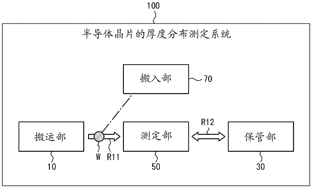
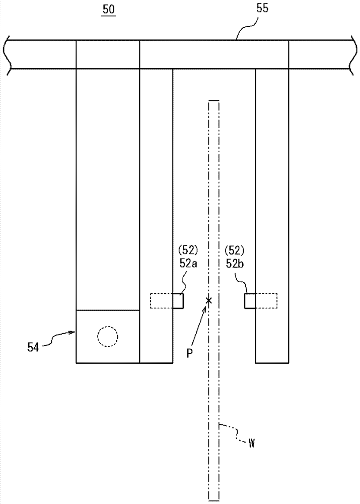
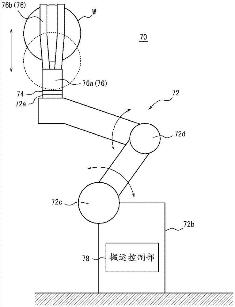
[0040] use figure 1 , FIGS. 3 to 5 illustrate a semiconductor wafer thickness distribution measurement system 100 according to an embodiment of the present invention. The semiconductor wafer polishing system 200 includes a loading unit 10, a storage unit 30, a measurement unit 50, and a transfer unit 70. The storage unit 30 stores the semiconductor wafer W in the storage unit 30, and the measurement unit 50 measures the thickness of the semiconductor wafer W. The transport unit 70 transports the semiconductor wafer W on the first transport route R11 between the loading unit 10 and the measurement unit 50 and the second transport route R12 between the storage unit 30 and the measurement unit 50 . Here, the conveyance unit 70 has a robot arm 72, a base 74, a robot arm 76, and a conveyance control unit 78. The robot arm 72 can move in the first conveyance path R11 and the second conveyance...

no. 2 Embodiment approach

[0063] (Second Embodiment: Semiconductor Wafer Polishing System)

[0064] use Figure 2~5A semiconductor wafer polishing system 200 according to one embodiment of the present invention will be described. The semiconductor wafer polishing system 200 includes a loading unit 10, a polishing unit 20, a storage unit 30, a measurement unit 50, and a transport unit 70. The loading unit 10 loads the semiconductor wafer W, the grinding unit 20 grinds the semiconductor wafer W, and the storage unit 30 stores For the semiconductor wafer W, the measuring section 50 measures the thickness distribution of the semiconductor wafer W, and the conveying section 70 passes through the first conveying path R21 between the carrying-in section 10 and the polishing section 20 of the measuring section 50, and the polishing section 20 and the measuring section respectively. The second conveyance path R22 between 50 conveys the semiconductor wafer W. Here, the transport unit 70 has a robot arm 72, a b...


PUM


Abstract

Herein, a thickness distribution measurement system, which can easily and high-precisely measure the thickness distribution of a semiconductor chip when a manipulator holds the semiconductor chip and can easily measures a semiconductor chip that is expanded towards a plurality of devices, is provided. The thickness distribution measurement system (100) includes a moving-in part (10), a storage part (30), a measuring part (50) and a moving part (70). The moving part (70) is provided with a manipulator (72), a bench (74) dipsosed on an end portion thereof, a manipulator (76) holding the semiconductor chip (W) and a moving control aprt (78). The measuring part (50) is provided with a measuring sensor (52), a linear scale (54), and a measuring control portion (56) that synchronizes the measurement values of moving distance of a rod (54R) and the thickness of the semiconductor chip (W), which is measured by the measuring sensor (52), in every time unit.

Description

technical field [0001] The present invention relates to a semiconductor wafer thickness distribution measurement system, a semiconductor wafer grinding system, a semiconductor wafer thickness distribution measurement method, a semiconductor wafer thickness margin distribution measurement method, and a semiconductor wafer grinding method. Background technique [0002] Semiconductor wafers such as silicon wafers are widely used as substrates of semiconductor devices. For example, a silicon wafer starts with the pulling process of a silicon single crystal ingot, goes through a slicing process, a surface grinding process, an etching process, and a grinding process, and is finally cleaned and processed into a polished wafer. In addition, silicon wafers are generally polished in multiple stages such as rough grinding and finish grinding, and semiconductor wafer polishing technology and semiconductor wafer thickness margin distribution measurement technology for confirming polishin...

Claims


Application Information

Patent Timeline
Patent Type & Authority Applications(China)
IPC IPC(8): B24B37/005B24B37/34B24B49/12B24B37/10H01L21/66
CPCB24B37/005B24B37/10B24B37/345B24B49/12H01L22/12H01L22/26
Inventor 大祥修
Owner SUMCO CORP
Why Eureka
Try Eureka