A display substrate and a display device

A technology for display substrates and thin film transistors, which is used in semiconductor/solid-state device parts, instruments, semiconductor devices, etc., and can solve problems such as inability to discharge static electricity, small relative area of ​​the display area of ​​the display substrate, and large wiring space.

Active Publication Date: 2019-03-15
BOE TECH GRP CO LTD +1
View PDF5 Cites 0 Cited by
  • Summary
  • Abstract
  • Description
  • Claims
  • Application Information

AI Technical Summary

Problems solved by technology

[0004] However, due to the large volume of the capacitor, in the existing display substrate design, the electrostatic discharge unit occupies a large wiring space, so that the relative area of ​​the display area of ​​the display substrate is relatively small, and the relative area of ​​the frame area is relatively large.
And, in the case of figure 1 In the electrostatic discharge unit shown, only the thin film transistor T is used for electrostatic discharge. Once the thin film transistor T is damaged, the electrostatic discharge unit will fail, making it impossible to discharge static electricity, which increases the risk of the display substrate being broken down by static electricity.
Therefore, how to reduce the large wiring space occupied by the electrostatic discharge unit and improve the reliability of the electrostatic discharge unit is a technical problem that those skilled in the art need to solve urgently

Method used


Image

  • A display substrate and a display device
  • A display substrate and a display device
  • A display substrate and a display device

Examples


Embodiment Construction

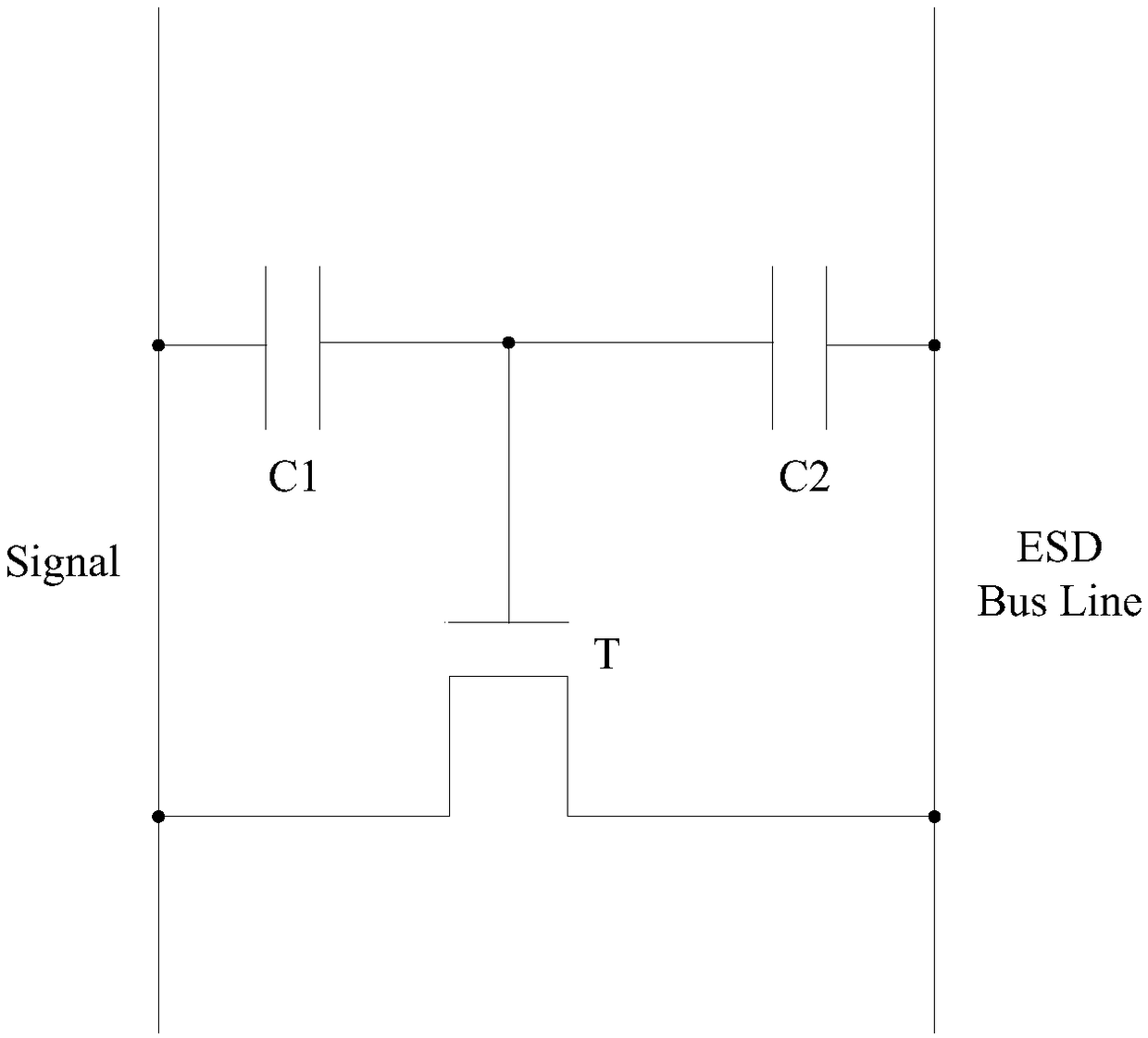
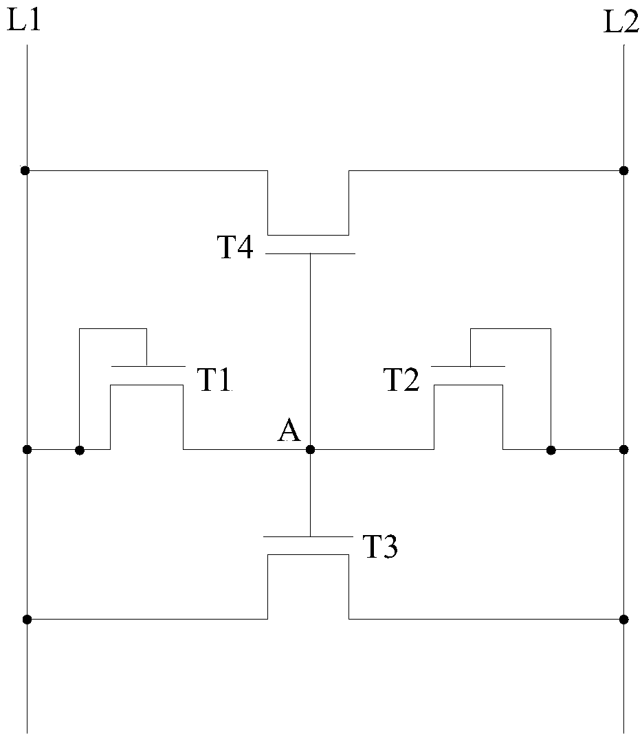
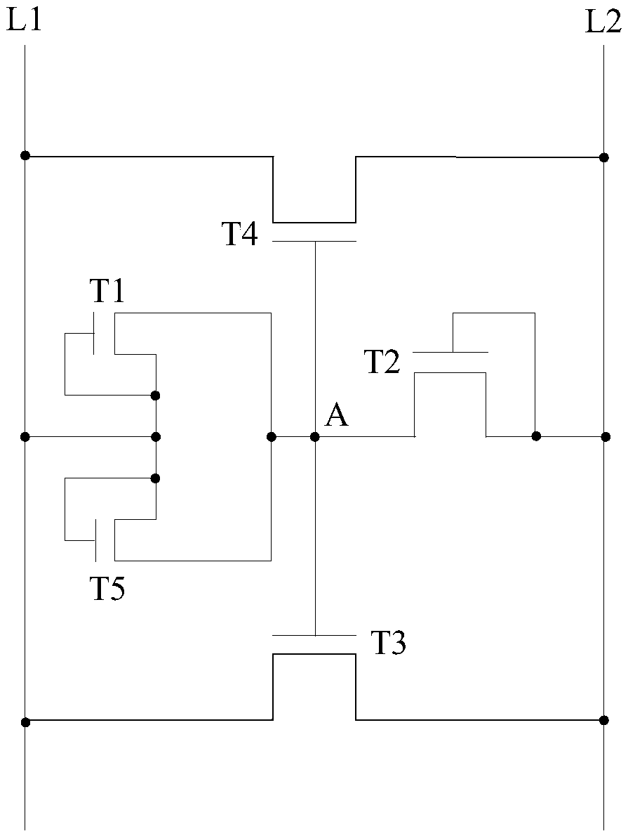
[0031] The specific implementation manners of the display substrate and the display device provided by the embodiments of the present invention will be described in detail below with reference to the accompanying drawings.

[0032] A display substrate provided by an embodiment of the present invention includes: a signal line arranged in the display area of ​​the display substrate, and an electrostatic discharge unit and an electrostatic lead-out line arranged in the frame area of ​​the display substrate, wherein,

[0033] Such as Figure 2 to Figure 5 As shown, the electrostatic discharge unit includes: a first thin film transistor T1, a second thin film transistor T2, a third thin film transistor T3 and a fourth thin film transistor T4;

[0034] The drain and the gate of the first thin film transistor T1 are respectively connected to the signal line L1;

[0035] The drain and the gate of the second thin film transistor T2 are respectively connected to the electrostatic lead-...


PUM


Abstract

The invention discloses a display substrate and a display device, comprising a signal line located in the display area of ​​the display substrate, an electrostatic lead-out line in the frame area, and a first thin film transistor, a second thin film transistor, a third thin film transistor and a fourth thin film transistor The electrostatic discharge unit; the drain and gate of the first thin film transistor are connected to the signal line; the drain and gate of the second thin film transistor are connected to the static electricity lead-out line; the source of the first thin film transistor and the source of the second thin film transistor pole, the gate of the third thin film transistor and the gate of the fourth thin film transistor are connected to the first node; the drain of the third thin film transistor and the drain of the fourth thin film transistor are connected to the signal line; the source of the third thin film transistor It is connected with the source electrode of the fourth thin film transistor and the electrostatic lead-out line. Since the electrostatic discharge unit includes four thin film transistors with small volume and discharges static electricity through the third and fourth thin film transistors, the wiring space thereof is reduced and the reliability thereof is improved.

Description

technical field [0001] The present invention relates to the field of display technology, in particular to a display substrate and a display device. Background technique [0002] The Electro-Static Discharge (ESD) unit is a thin film transistor liquid crystal display substrate (Thin Film Transistor-Liquid Crystal Display, TFT-LCD) and an active matrix organic electroluminescent display substrate (Active-Matrix Organic Light Emitting Diode, AMOLED )important parts of. The electrostatic discharge unit is used to reduce electrostatic damage to the display substrate during the manufacturing process of the display substrate, such as developing, etching, and module bonding (Bonding), so as to improve the yield of the display substrate. [0003] Such as figure 1 As shown, the electrostatic discharge unit in the prior art is composed of two capacitors C1, C2 and a thin film transistor T. When a large amount of static electricity accumulates on the signal line of the signal termina...

Claims


Application Information

Patent Timeline
Patent Type & Authority Patents(China)
IPC IPC(8): G02F1/1362H01L27/32
CPCG02F1/136204H01L27/1285H01L27/124H01L23/60H01L27/0266H01L27/1262
Inventor 王迎李红敏廖力勍孙丽
Owner BOE TECH GRP CO LTD
Why Eureka
Try Eureka