Method for manufacturing optical compound film structure with controllable transparency pattern changes

An optical composite film and manufacturing method technology, applied in optics, nonlinear optics, instruments, etc., can solve the problems of long production cycle, inability to achieve continuous production, high production cost, etc.

Inactive Publication Date: 2017-08-15
NANOBIT TECH
View PDF5 Cites 15 Cited by
  • Summary
  • Abstract
  • Description
  • Claims
  • Application Information

AI Technical Summary

Problems solved by technology

However, the existing process can only be applied to the processing of sheet-like PDLC composite layers, and cannot achieve the efficiency of continuous production, resulting in higher production costs and longer production cycles

Method used


Image

  • Method for manufacturing optical compound film structure with controllable transparency pattern changes
  • Method for manufacturing optical compound film structure with controllable transparency pattern changes
  • Method for manufacturing optical compound film structure with controllable transparency pattern changes

Examples


no. 1 example

[0027] see figure 1 , is a schematic flowchart of the manufacturing method of the optical composite film structure capable of controlling the change of the light transmission pattern according to the first embodiment of the present invention. And please refer to Figure 2A to Figure 9 , is a process schematic diagram corresponding to the manufacturing method of this embodiment.

[0028] The manufacturing method of this embodiment is suitable for manufacturing an optical composite film structure with a polymer dispersed liquid crystal (PDLC) layer, wherein the polymer dispersed liquid crystal layer is formed with a conductive circuit pattern and a lead circuit, and the lead circuit can be connected to the outside through the wiring. The control unit is electrically connected, so the optical composite film structure can pass through the control unit to make the area on the polymer dispersed liquid crystal layer related to the conductive circuit pattern produce a partial light t...

no. 2 example

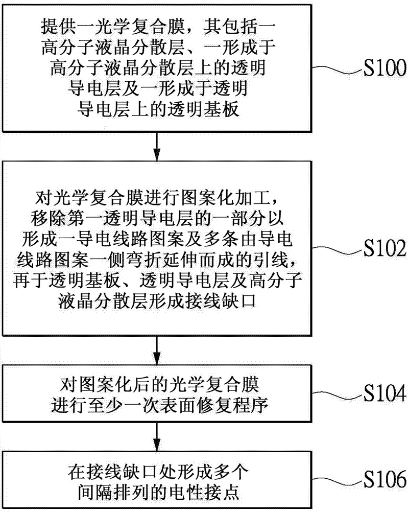
[0042] see Figure 10 , is a schematic flowchart of the manufacturing method of the optical composite film structure capable of controlling the change of the light transmission pattern according to the second embodiment of the present invention. Such as Figure 10 As shown, the manufacturing method of this embodiment includes: Step S200, providing an optical composite film, which includes a polymer liquid crystal dispersion layer, a transparent conductive layer formed on the polymer liquid crystal dispersion layer, and a transparent conductive layer formed on the transparent conductive layer. a transparent substrate; step S202, performing at least one surface repair procedure on the optical composite film; step S204, patterning the surface repaired optical composite film, removing a part of the first transparent conductive layer to form a conductive circuit pattern and A plurality of lead wires formed by bending and extending one side of the conductive circuit pattern, and th...


PUM

PropertyMeasurementUnit
thicknessaaaaaaaaaa
thicknessaaaaaaaaaa
thicknessaaaaaaaaaa

Abstract

The invention provides a method for manufacturing an optical composite membrane structure capable of controlling a change in light transmission pattern includes the steps of first providing an optical composite film comprising a polymer liquid crystal dispersion layer, a transparent conductive layer formed on the polymer liquid crystal dispersion layer, Transparent conductive layer; and then, the optical composite film is patterned to remove portions of the transparent conductive layer to form a conductive line pattern and a plurality of leads extending from the conductive line pattern side, and forming a transparent substrate A transparent substrate, a transparent conductive layer and a polymer liquid crystal dispersion layer; and then, at least a sub-surface repair program for the patterned optical composite film; and finally, an electrical contact is formed at the wiring gap.

Description

technical field [0001] The invention relates to a manufacturing method of an optical composite film, in particular to a manufacturing method of an optical composite film structure capable of controlling the change of a light transmission pattern. Background technique [0002] Polymer Dispersed Liquid Crystal (PDLC) is composed of submicron-sized liquid crystal particles (Liquid Crystal droplet) uniformly dispersed in the polymer material, because it "can use an external electric field to operate in the state of light scattering or light Therefore, it can be used on conductive glass, such as encapsulating PDLC in conductive glass, so that the change of the electric field (switch) can be used to make the light-transmitting structure appear transparent or opaque. The conductive glass used to build PDLC is called Smart Windows in the market. [0003] With the upgrading of process technology and materials, the applicability of PDLC has been greatly improved. For example, soft co...

Claims


Application Information

Patent Timeline
Patent Type & Authority Applications(China)
IPC IPC(8): G02F1/1334G02F1/13G02F1/1343
CPCG02F1/13G02F1/1334G02F1/1343G02F1/13439G02F1/1316
Inventor 张裕洋刘修铭谷福田陈家庆丁定国
Owner NANOBIT TECH
Why Eureka
Try Eureka