Structure and process for realizing WLCSP six-side plastic sealing of TVS chip

A chip and process technology, applied in the field of semiconductor packaging, can solve problems that affect the reliability of electronic products, difficult side insulation protection, chip side pollution, etc., achieve low cost, improve product performance, and simple process flow

Inactive Publication Date: 2017-08-18
SHANGHAI CHANGYUAN WAYON MICROELECTRONICS
View PDF3 Cites 1 Cited by
  • Summary
  • Abstract
  • Description
  • Claims
  • Application Information

AI Technical Summary

Problems solved by technology

It is difficult to achieve insulation protection on the side
However, in the application of ultra-small package TVS products, such as DFN1006, DFN0603 or even DFN0402, it is found that in the production of SMT chips, due to the control accuracy of most SMT equipment for solder, and when the robot arm or manual grabbing chip The problem of control accuracy may cause solder to contaminate the side of the chip, which will lead to serious situations such as short circuit of electronic products, and affect the reliability of electronic products

Method used


Image

  • Structure and process for realizing WLCSP six-side plastic sealing of TVS chip
  • Structure and process for realizing WLCSP six-side plastic sealing of TVS chip
  • Structure and process for realizing WLCSP six-side plastic sealing of TVS chip

Examples


Embodiment Construction

[0030] The technical solutions of the present invention will be described in detail below with reference to the accompanying drawings.

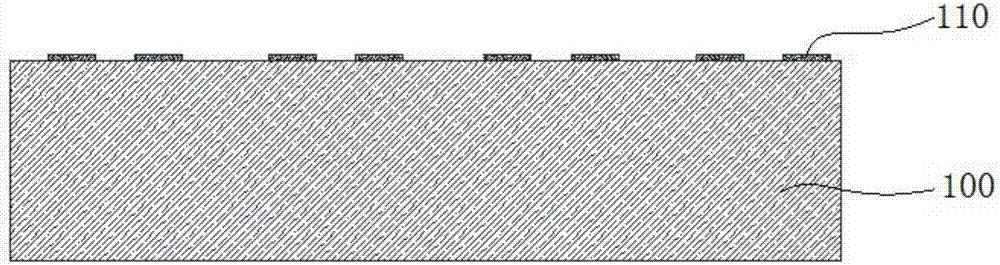
[0031] like image 3 A cross-sectional view of the wafer 100 is shown, and the metal region 110 is the region where the front side of the wafer serves as an electrode;

[0032] like Figure 4 As shown, as in the conventional WLCSP process, metal bumps 120 are first prepared on the front side of the wafer (pillar process).

[0033] like Figure 5 As shown, according to the structure of the final TVS product, the wafer is cut to prepare the gap 130, and the depth of the gap is controlled during cutting, and the wafer cannot be cut through;

[0034] The above steps can obtain the aforementioned TVS chip structure for realizing WLCSP six-sided plastic packaging.

[0035] like Image 6 As shown, the plastic encapsulation is completed from the front side of the wafer downward to obtain a front plastic encapsulation 140 covering the gap 130 obt...


PUM


Abstract

The invention discloses a structure and process for realizing WLCSP six-side plastic sealing of a TVS chip and is same as the routine WLCSP process. The process comprises steps that firstly, metal convex points are prepared at a front surface of a wafer; the wafer is cut to prepare a gap according to a final TVS product structure, depth of the gap is controlled during cutting, and the wafer can not be cut through; first plastic sealing is carried out from the front surface of the wafer, and the gap acquired through cutting is covered; wafer thinning is carried out from the front surface of the wafer, and an electrode is guaranteed to expose; if the electrode need be higher than a plastic sealing surface, the primary planting or coating process is carried out at the metal convex point portion; wafer thinning is carried out at a back surface of the wafer till size requirements of the final TVS product are satisfied; plastic sealing is carried out for the back surface of the wafer, and protection of the back surface of the wafer is accomplished; cutting is carried out along the center of the gap, through cutting is realized, and chip separation is accomplished. The method is advantaged in that the process flow is simple, process control requirements are not high, and thickness of finished products can be controlled for being quite thin.

Description

technical field [0001] The invention relates to the technical field of semiconductor packaging, in particular to a WLCSP six-sided plastic packaging structure and process for ultra-small packaging TVS products. Background technique [0002] As a new type of packaging technology, WLCSP (Wafer Level Chip Scale Packaging) technology has been mass-produced in many products. The biggest feature of this process is that it does not require a lead frame to fix the chip, nor does it require connection means such as wirebonding. Instead, the pillar is directly processed on the wafer level. The material of the pillar can be gold, copper or alloy materials. Then directly realize chip programming and testing through wafer sort. [0003] Compared with the traditional packaging process, the WLCSP process has the advantages of simple process flow, few steps, low cost and high production efficiency. In particular, there is no need to use a lead frame, so the chip size and shape can have a...

Claims


Application Information

Patent Timeline
Patent Type & Authority Applications(China)
IPC IPC(8): H01L23/31H01L23/498H01L21/48H01L21/56
CPCH01L23/49816H01L23/49838H01L21/4853H01L21/56H01L23/3114H01L23/3128
Inventor 吴昊余晓明
Owner SHANGHAI CHANGYUAN WAYON MICROELECTRONICS
Why Eureka
Try Eureka