Method for producing connected body, method for connecting electronic parts, connected body

A manufacturing method and technology of electronic components, applied in adhesive heating bonding method, semiconductor/solid-state device manufacturing, bonding method, etc., can solve high thermal pressing temperature, uneven display, large thermal shock, etc. question

Active Publication Date: 2020-03-03
DEXERIALS CORP
View PDF9 Cites 0 Cited by
  • Summary
  • Abstract
  • Description
  • Claims
  • Application Information

AI Technical Summary

Problems solved by technology

[0008] However, in such a connection method using an anisotropic conductive film, the thermal press temperature is high, and the thermal shock to electronic components such as the IC 115 for liquid crystal driving or the transparent substrate 103 becomes large.
Furthermore, after the anisotropic conductive film is connected, when the temperature drops to normal temperature, the adhesive shrinks due to the temperature difference, and warpage may occur at the terminal portion 109a of the transparent substrate 103
Therefore, there is a possibility of causing defects such as display unevenness or poor connection of the IC 115 for liquid crystal driving.

Method used


Image

  • Method for producing connected body, method for connecting electronic parts, connected body
  • Method for producing connected body, method for connecting electronic parts, connected body
  • Method for producing connected body, method for connecting electronic parts, connected body

Examples


no. 1 Embodiment approach >

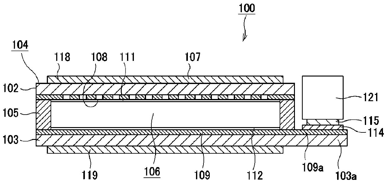
[0048] In the following first embodiment, a case of so-called COG (chip on glass) mounting in which an IC chip for driving a liquid crystal is mounted as an electronic component on a glass substrate of a liquid crystal display panel will be described as an example. The liquid crystal display panel 10, such as figure 1 As shown, two transparent substrates 11 , 12 made of glass substrates or the like are arranged facing each other, and these transparent substrates 11 , 12 are bonded to each other by a frame-shaped sealing material 13 . Further, in the liquid crystal display panel 10 , a panel display portion 15 is formed by enclosing liquid crystal 14 in a space surrounded by the transparent substrates 11 and 12 .

[0049] A pair of stripe-shaped transparent electrodes 16 and 17 made of ITO (indium tin oxide) or the like are formed on both inner surfaces of the transparent substrates 11 and 12 facing each other so as to cross each other. Then, the two transparent electrodes 16...

specific example 1-1

[0069] [Temporary pasting process]

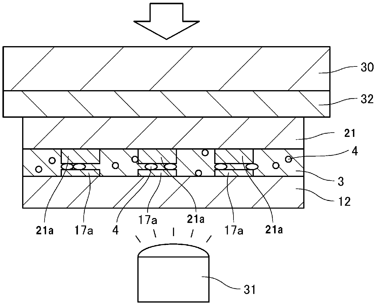
[0070] First, the anisotropic conductive film 1 is temporarily pasted on the transparent substrate 12 (adhesive placement step). A method of temporarily pasting an anisotropic conductive film such as image 3 As shown, the anisotropic conductive film 1 is disposed on the transparent electrode 17 of the transparent substrate 12 so that the adhesive resin layer 3 faces the transparent electrode 17 side. After disposing the adhesive resin layer 3 on the transparent electrode 17, heat and press the adhesive resin layer 3 from the release film 2 side with a thermocompression bonding tool, for example, to separate the thermocompression bonding tool from the release film 2. , the release film 2 is peeled from the adhesive resin layer 3 . In addition, the temporary bonding of the anisotropic conductive film 1 may be performed by pressurization and light irradiation of a thermocompression bonding tool, and may be performed using thermocompression ...

specific example 1-2

[0086] In this manufacturing method, ultraviolet irradiation may be performed from the IC 18 side for liquid crystal driving instead of the ultraviolet irradiation from the transparent substrate 12 side in the temporary pressure-bonding process described above.


PUM

PropertyMeasurementUnit
diameteraaaaaaaaaa
heightaaaaaaaaaa
thicknessaaaaaaaaaa

Abstract

By using a photocurable adhesive, electronic components are connected at low temperature, and misalignment of electronic components is prevented. It has: an adhesive arrangement process of providing the circuit connection adhesive 1 containing a photopolymerization initiator on the transparent substrate 12; disposing the electronic component 18 on the transparent substrate 12 via the circuit connection adhesive 1, and performing Temporary pressure-bonding process of pressing the electronic component 18 to the transparent substrate 12 and irradiating the circuit-connecting adhesive 1 with light; and a main pressure-bonding process of heating and irradiating the electronic component 18 against the transparent substrate , the amount of light irradiation in the provisional pressure-bonding process is smaller than the light irradiation amount in the main pressure-bonding process.

Description

technical field [0001] The present invention relates to a method for producing a connecting body in which an electronic component is connected to a transparent substrate via an adhesive for circuit connection containing a photopolymerization initiator, and for connecting an electronic component to a transparent substrate via an adhesive for circuit connection containing a photopolymerization initiator The above connection method and the connection body manufactured using this method. This application claims priority based on Japanese Application No. 2015-8950 filed in Japan on January 20, 2015 and Japanese Application No. 2016-8718 filed in Japan on January 20, 2016. These applications This application is incorporated by reference. Background technique [0002] Conventionally, liquid crystal display devices have been frequently used as various display units such as televisions, PC monitors, mobile phones, portable game machines, tablet PCs, and vehicle-mounted monitors. In...

Claims


Application Information

Patent Timeline
Patent Type & Authority Patents(China)
IPC IPC(8): H01L21/60C09J5/00C09J5/06C09J9/02C09J11/06C09J201/02H05K3/32
CPCH01L2224/73204H01L2224/81H01L2224/83192C09J5/06H05K3/32
Inventor 梶谷太一郎平尾未希
Owner DEXERIALS CORP
Why Eureka
Try Eureka