AIN epitaxial thin film preparation method

A technology of epitaxial film and nucleation layer, which is applied in semiconductor/solid-state device manufacturing, coating, gaseous chemical plating, etc., can solve the problem of high dislocation density of AlN film and achieve low dislocation density effect

Inactive Publication Date: 2017-08-22
PEKING UNIV
View PDF3 Cites 16 Cited by
  • Summary
  • Abstract
  • Description
  • Claims
  • Application Information

AI Technical Summary

Problems solved by technology

[0006] One purpose of the embodiments of the present invention is to solv...

Method used


Image

  • AIN epitaxial thin film preparation method
  • AIN epitaxial thin film preparation method
  • AIN epitaxial thin film preparation method

Examples


preparation example Construction

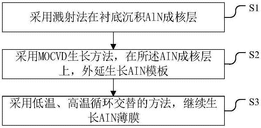
[0031] figure 1 It shows a schematic flow chart of a method for preparing an AlN epitaxial thin film provided by an embodiment of the present invention, see figure 1 , the method specifically includes the following steps:

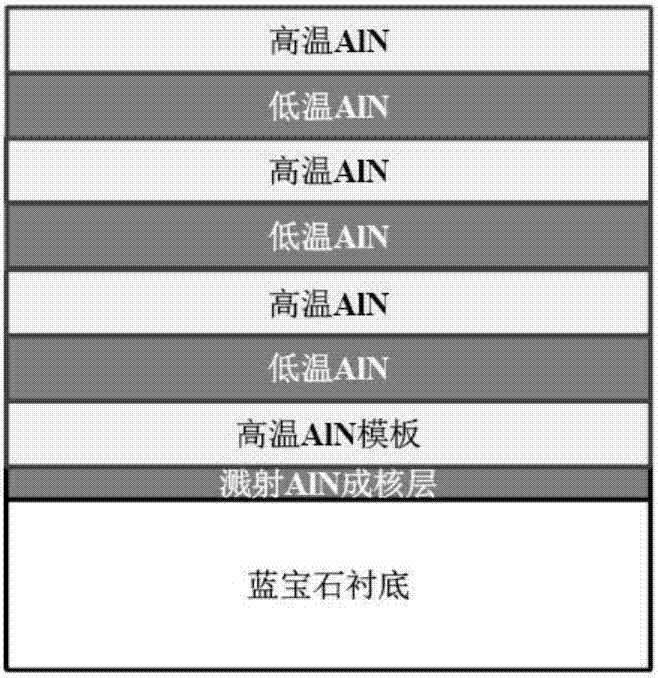
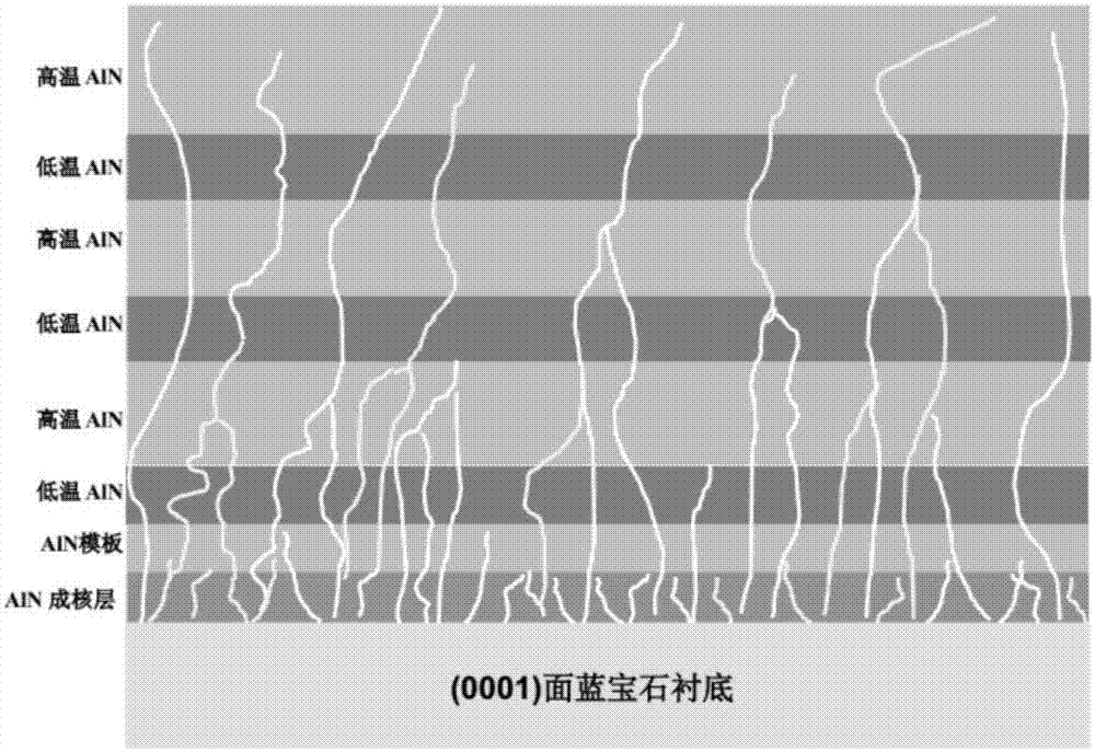
[0032] S1. Depositing an AlN nucleation layer on the cleaned c-plane sapphire substrate by sputtering;

[0033] S2. Using the MOCVD growth method to epitaxially grow an AIN template on the AIN nucleation layer;

[0034] S3. Continue to grow the AIN thin film by adopting the low temperature and high temperature cycle alternating method.

[0035] Steps S1-S3 are described in detail below:

[0036] In the step S1, the thickness of the nucleation layer is 5-400nm, and the substrate temperature is 300-900°C.

[0037] Described step S2 comprises:

[0038] Passing hydrogen gas into the reaction chamber of the MOCVD equipment where the substrate is placed, keeping the temperature in the reaction chamber at 1200-1250°C and the pressure at 50-100mbar;

[0039] ...


PUM


Abstract

The embodiment of the invention discloses a method for preparing an AlN epitaxial film. The method includes: S1, depositing an AlN nucleation layer on a substrate by a sputtering method; S2, epitaxially growing an AIN template on the AlN nucleation layer by using an MOCVD growth method; S3, adopting a method of alternating low temperature and high temperature cycles, Continue to grow the AIN thin film. In the embodiment of the present invention, a layer of AlN is first sputtered by sputtering, and then the AlN film is grown by temperature modulation growth in MOCVD. Compared with the prior art, the AlN film with atomically smooth surface and low dislocation density can be prepared. .

Description

technical field [0001] The embodiment of the present invention relates to the technical field of preparation of III-nitride wide bandgap semiconductors, and specifically relates to a method for preparing an AlN epitaxial film. Background technique [0002] In recent years, the rapid development of information science and technology has promoted the exploration of III-nitride semiconductor materials and devices in the direction of low power consumption, multi-band, ultra-fast response, ultra-high capacity, miniaturization, and high integration. AlGaN material has the characteristics of direct bandgap and its forbidden band width can be continuously adjusted from 3.4eV (365nm) to 6.2eV (200nm) with different Al components. In addition, due to its low surface recombination rate, high quantum efficiency, and high stability in harsh environments, AlGaN and its low-dimensional quantum well structure are also suitable for preparing short-wavelength deep ultraviolet light-emitting d...

Claims


Application Information

Patent Timeline
IPC IPC(8): C23C16/34C23C16/02H01L21/02
CPCC23C16/303C23C16/0272H01L21/0242H01L21/02458H01L21/0254H01L21/0262
Inventor 许福军沈波张立胜王明星解楠秦志新于彤军王新强
Owner PEKING UNIV
Why Eureka
Try Eureka