Broadband active inductor with high Q values and coarsely tunable and finely tunable inductance value

A technology of active inductance and inductance value, which is applied in the direction of analog reactance network, single-port active network, network using active components, etc. It can solve the problem of low Q value at high frequency, single tuning method, center frequency drift, etc. problem, to achieve the effect of high output impedance, large Q value and bandwidth, small equivalent series resistance and zero frequency

Active Publication Date: 2017-09-01
BEIJING UNIV OF TECH
View PDF6 Cites 9 Cited by
  • Summary
  • Abstract
  • Description
  • Claims
  • Application Information

AI Technical Summary

Problems solved by technology

[0004] However, due to the simple circuit topology and single tuning method of current active inductors, there are small inductance values ​​and low Q values ​​at high frequencies, and the tuning of inductance values ​​and Q is relatively rough and not fine enough. There are still some deficiencies in multi-band LC voltage-controlled oscillators and LC active band-pass filters
For example: In a multi-band VCO, it is hoped that the oscillation frequency can be adjusted in a wide range, and there is a high Q value at the oscillation frequency, which requires the active inductor to have a wide inductance value and Q value tuning capability; in the LC active bandpass In the filter, small changes in noise, temperature, voltage, etc. will often cause the center frequency to drift, which requires fine adjustment of the inductance value. Tuning, as well as high Q value at high frequencies and tuning performance over a wide frequency range

Method used


Image

  • Broadband active inductor with high Q values and coarsely tunable and finely tunable inductance value
  • Broadband active inductor with high Q values and coarsely tunable and finely tunable inductance value
  • Broadband active inductor with high Q values and coarsely tunable and finely tunable inductance value

Examples


Embodiment Construction

[0018] In order to make the object, technical solution and advantages of the present invention clearer, the present invention will be further described below in conjunction with the accompanying drawings.

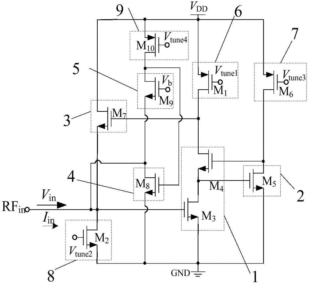
[0019] figure 1 is an embodiment of the new active inductor. Including: a first transconductance unit (1), a modulation unit (2), a second transconductance unit (3), a third transconductance unit (4), a fourth transconductance unit (5), a first adjustable bias A circuit (6), a second adjustable bias circuit (7), a third adjustable bias circuit (8), and a fourth adjustable bias circuit (9).

[0020] In the embodiment of the novel active inductor, the first transconductance unit (1) includes a third N-type MOS transistor (M 3 ), the fourth N-type MOS transistor (M 4 ); Modulation unit (2) is the fifth N-type MOS transistor (M 5 ); the second transconductance unit (3) is the seventh N-type MOS transistor (M 7 ); the third transconductance unit (4) is the eighth N-type MOS...


PUM


Abstract

The invention discloses a broadband active inductor with high Q values and a coarsely tunable and finely tunable inductance value. The broadband active inductor comprises a first transconductance unit (1), a modulation unit (2), a second transconductance unit (3), a third transconductance unit (4), a fourth transconductance unit (5), a first tunable bias circuit (6), a second tunable bias circuit (7), a third tunable bias circuit (8) and a fourth tunable bias circuit (9). The modulation unit is connected with the first transconductance unit and is used for increasing the Q values and bandwidth of the active inductor. The first transconductance unit, the modulation unit and the second transconductance unit form a master circuit. The third transconductance unit and the fourth transconductance unit form a slave circuit. The master circuit and the slave circuit are connected in parallel. The equivalent capacitance for synthesizing the inductance in the whole circuit is increased, so the inductance value of the active inductor is improved. According to the active inductor, the high Q peaks of the active inductor under different frequencies are realized, the Q peaks can be tuned, and the inductance value of the active inductor is coarsely tuned and finely tuned.

Description

technical field [0001] The invention relates to the field of radio frequency devices and integrated circuits, in particular to a high quality factor Q peak value that can be tuned at different frequencies, and the inductance value can be roughly adjusted in a large range and in a small range. Novel Broadband Tunable Active Inductors for Fine Tuning. Background technique [0002] With the application and proposal of the fourth and fifth generation mobile communications, global long-distance communications and high-speed wireless data transmission have brought about a revolution in mobile terminals. The development of various wireless communication standards not only requires RF transceivers to meet the requirements of full integration, miniaturization, tunable performance, and low power consumption, but also puts forward new requirements for multi-mode and multi-band RF transceivers. Radio frequency integrated circuits such as LC active band-pass filters and LC voltage-contr...

Claims


Application Information

Patent Timeline
Patent Type & Authority Applications(China)
IPC IPC(8): H03H11/48
CPCH03H11/486
Inventor 张万荣杨坤谢红云金冬月吕晓强王娜温晓伟郭燕玲孙丹陈吉添黄鑫
Owner BEIJING UNIV OF TECH
Why Eureka
Try Eureka