

Reflow SMT Process
A reflow soldering and reflow soldering technology, applied in the direction of assembling printed circuits with electrical components, can solve the problems of reducing the reliability of the device, excessive contact resistance, and reducing the safe working area of the device, and achieve the effect of reducing the generation of water vapor
- Summary
- Abstract
- Description
- Claims
- Application Information
AI Technical Summary
Problems solved by technology
Method used
Image

Examples
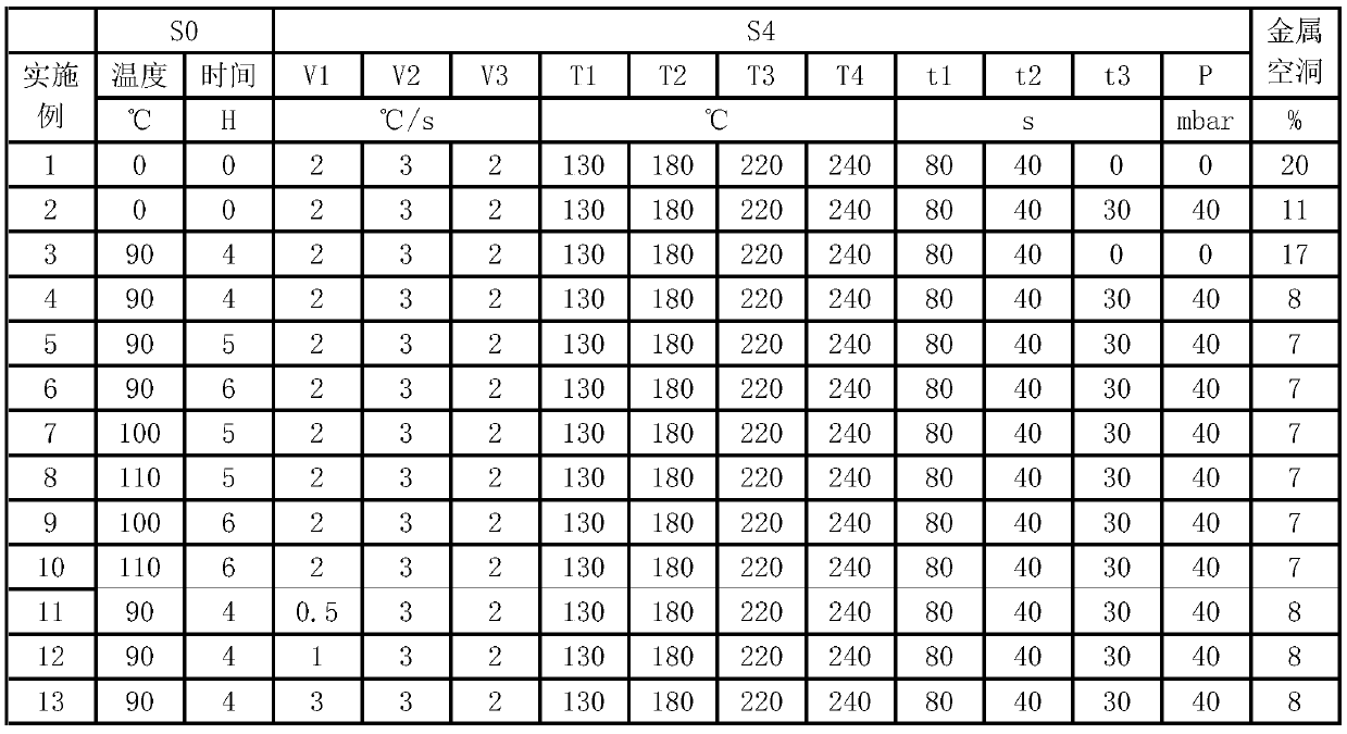
Embodiment 1-56
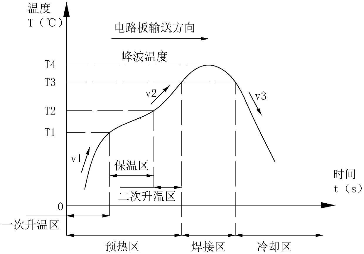
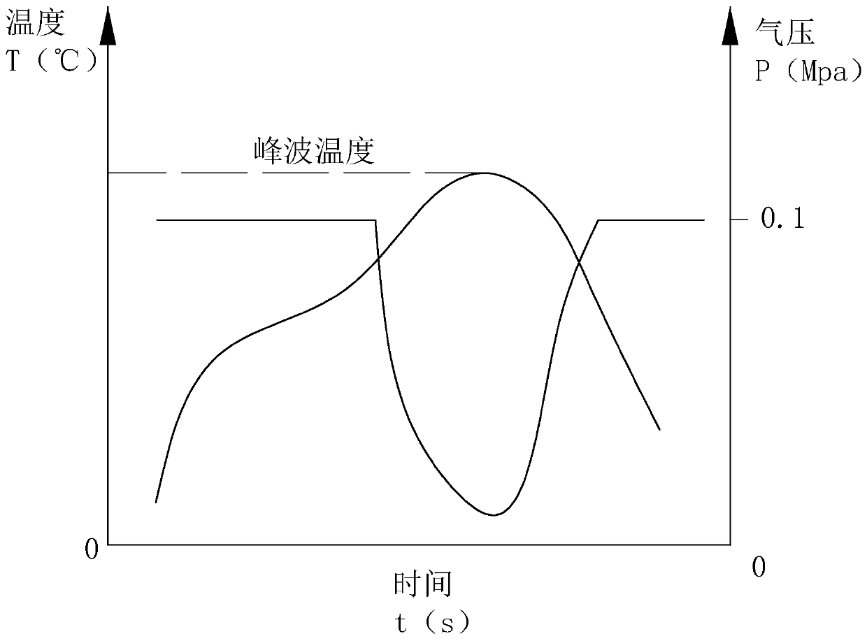
[0036] Embodiment 1-56: a reflow soldering patch process, comprising the following steps:
[0037] S0, drying, sending the circuit board to be soldered into an oven for pre-baking for 4-6H, and the drying temperature is 90-110°C;
[0038] S1. Printing solder paste. After the circuit board is detected correctly by the optical camera, the circuit board is pasted under the stencil, and the solder paste is passed through the mesh on the stencil while the lead-free scraper is moving above the stencil. The solder paste is printed on the circuit board through the hole, and the solder paste is Sn-Ag-Cu alloy solder. The mesh on the stencil is an inverted tapered round hole to increase the surface area of the solder paste printed on the circuit board. ;
[0039] S2, placement, sending the circuit board after step S1 into the placement machine for placement;
[0040] S3. Intermediate inspection, check whether the polarity of the component is reversed, whether the mounting is offset,...
PUM
 Abstract
Description
Claims
Application Information