Thin film transistor, manufacturing method of thin film transistor and display substrate

A technology of thin film transistors and manufacturing methods, applied in the direction of transistors, semiconductor/solid-state device manufacturing, semiconductor devices, etc., can solve the problems of easy corrosion of the active layer, affecting the driving performance of TFT, and damage to the conductive channel, so as to improve the driving performance. Performance, small conduction resistance, effect of reducing contact resistance

Active Publication Date: 2017-09-05
BOE TECH GRP CO LTD
View PDF2 Cites 4 Cited by
  • Summary
  • Abstract
  • Description
  • Claims
  • Application Information

AI Technical Summary

Problems solved by technology

[0005] In order to solve the problem that in the process of forming the source and drain electrodes in the TFT by etching in the related art, the part of the active layer in contact with the etching solution is easily corroded, resulting in damage to the conductive channel in the active layer, thereby affecting the For the problem of driving performance of TFT, an embodiment of the present invention provides a thin film transistor, a manufacturing method thereof, and a display substrate

Method used


Image

  • Thin film transistor, manufacturing method of thin film transistor and display substrate
  • Thin film transistor, manufacturing method of thin film transistor and display substrate
  • Thin film transistor, manufacturing method of thin film transistor and display substrate

Examples


Embodiment Construction

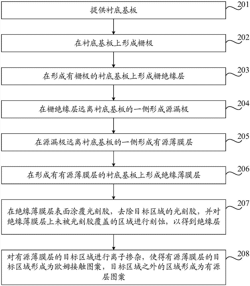
[0042] In order to make the object, technical solution and advantages of the present invention clearer, the implementation manner of the present invention will be further described in detail below in conjunction with the accompanying drawings.

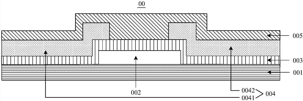
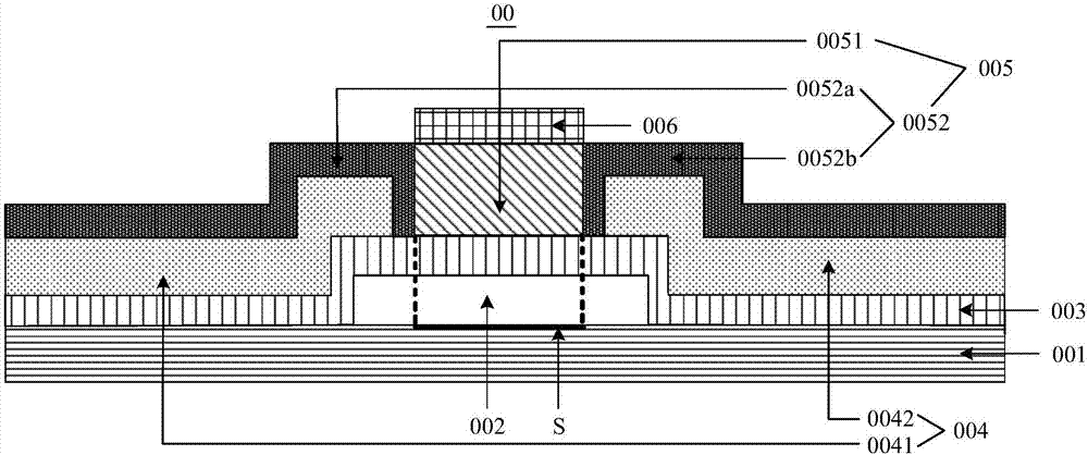
[0043] figure 1 is a schematic structural diagram of a thin film transistor 00 provided by an embodiment of the present invention, as shown in figure 1 As shown, the thin film transistor 00 may include:

[0044] The gate electrode 002 and the gate insulating layer 003 provided on the base substrate 001 are stacked in this order.

[0045] The side of the gate insulating layer 003 away from the base substrate 001 is provided with a source and drain 004 , and the source and drain 004 includes a source 0041 and a drain 0042 .

[0046] An active layer 005 is provided on the side of the source and drain electrodes 004 away from the base substrate 001 , and the active layer 005 is connected to the source electrode 0041 and the drain electro...


PUM


Abstract

The invention discloses a thin film transistor, a manufacturing method of the thin film transistor and a display substrate and belongs to the technical field of display. The thin film transistor comprises a grid electrode and a grid insulation layer which are sequentially stacked on the lining substrate. A source and drain electrode is arranged on the side, away from the lining substrate, of the grid insulation layer and comprises a source electrode and a drain electrode. An active layer is arranged on the side, away from the lining substrate, of the source and drain electrode and is connected with the source electrode and the drain electrode. According to the thin film transistor, the manufacturing method of the thin film transistor and the display substrate, contact of the active layer and etching liquid is avoided in the source and drain electrode forming process, damage of conductive channels in the active layer can be avoided in the process, and influences on the driving performance of the TFT is avoided. The thin film transistor, the manufacturing method of the thin film transistor and the display substrate are used for displaying images.

Description

technical field [0001] The invention relates to the field of display technology, in particular to a thin film transistor, a manufacturing method thereof, and a display substrate. Background technique [0002] A thin film transistor (English: Thin Film Transistor; abbreviation: TFT) includes a layered structure such as a gate, a gate insulating layer, an active layer, a source and a drain, and an insulating layer that are sequentially stacked on a substrate, wherein the source and drain include source and drain. [0003] When using related technologies to manufacture thin film transistors, after the active layer is formed, a whole layer of metal film layer is formed on the substrate on which the active layer is formed, and then the whole layer is formed by wet etching process. The metal film layer is etched to form source and drain electrodes with a certain pattern. [0004] During the etching process, the part of the active layer in contact with the etchant is easily corro...

Claims


Application Information

Patent Timeline
Patent Type & Authority Applications(China)
IPC IPC(8): H01L29/786H01L29/45H01L21/336
CPCH01L29/45H01L29/458H01L29/66765H01L29/786H01L29/7866H01L29/7869
Inventor 薛大鹏
Owner BOE TECH GRP CO LTD
Why Eureka
Try Eureka