Plasma processing device and method

A plasma and processing device technology, applied in the field of semiconductor manufacturing and ion processing device internal cleaning, can solve the problems of reducing equipment cleaning efficiency, difficult to ensure consistent substrate process environment, poor component cleaning effect, etc., to ensure cleaning effect, The effect of avoiding discharge and increasing concentration

Active Publication Date: 2017-09-12
ADVANCED MICRO FAB EQUIP INC CHINA
View PDF7 Cites 11 Cited by
  • Summary
  • Abstract
  • Description
  • Claims
  • Application Information

AI Technical Summary

Problems solved by technology

In the capacitively coupled plasma reaction device, since the cleaning plasma is generated by the electric field between the upper electrode and the lower electrode, due to the uneven distribution of the electric field lines between the upper electrode and the lower electrode, the edge region is generated The plasma concentration is lower than the plasma concentration generated in the central area, so the cleaning effect of the components in the edge area of ​​the reaction chamber is not good, the cleaning efficiency of the equipment is reduced, and it is difficult to ensure that the process environment of each substrate is consistent

Method used


Image

  • Plasma processing device and method
  • Plasma processing device and method
  • Plasma processing device and method

Examples


Embodiment Construction

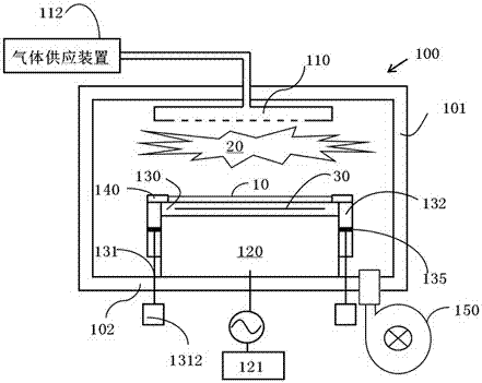
[0026] The specific embodiments of the present invention will be described below in conjunction with the accompanying drawings. The technology disclosed in the present invention is applicable to various plasma processing devices, especially suitable for capacitively coupled plasma processing devices.

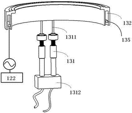
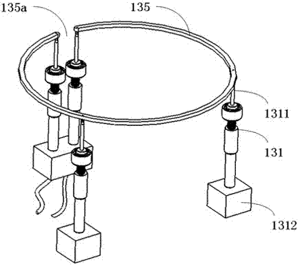
[0027] figure 1 A schematic structural diagram of an ion plasma treatment device applicable to the method of the present invention is shown. In this embodiment, the plasma processing device is a capacitively coupled plasma processing device, and the capacitively coupled plasma processing device includes a reaction chamber 100, and the reaction chamber includes a substantially cylindrical reaction chamber side wall made of a metal material 101 and the reaction chamber bottom wall 102, the reaction chamber side wall 101 and the reaction chamber bottom wall 102 and the reaction chamber upper wall form a reaction chamber structure that can be vacuumed, and an upper electrode 110 is...


PUM


Abstract

The invention provides a plasma processing device and a method of processing a substrate in the plasma processing device. The plasma processing device comprises a reaction chamber in which an upper electrode and a lower electrode are arranged. A hollow insulating ring is arranged around the periphery of the lower electrode and is internally provided with a radio frequency coil, and by applying radio frequency power to the radio frequency coil in the cleaning process, the degree of dissociation of the cleaning gas in the edge area can be improved, thereby increasing the concentration of the clean plasma in the edge area. The clean plasma of the high concentration is beneficial for ensuring the clean effect of the component in the edge area. In the etching, the radio frequency coil is grounded to effectively avoid a phenomenon that the radio frequency power applied to the lower electrode produces discharge in the radio frequency coil.

Description

technical field [0001] The invention relates to the field of semiconductor manufacturing, in particular to the technical field of internal cleaning of a plasma processing device. Background technique [0002] Plasma reaction devices are widely used in the manufacturing process of integrated circuits, such as deposition and etching. Among them, commonly used plasma etching reaction devices include capacitively coupled plasma reaction device CCP and inductively coupled plasma device ICP. The principle of plasma reaction device is mainly to use radio frequency power to dissociate the reaction gas input into the reaction device into Plasma, which is used to perform plasma etching on the substrate placed inside it. The etching process of different substrates requires different reaction gases, and also produces different reaction by-products. Some reaction by-products React with each other and deposit on the inner side wall of the reaction chamber or other components, affecting t...

Claims


Application Information

Patent Timeline
Patent Type & Authority Applications(China)
IPC IPC(8): H01J37/32
CPCH01J37/32477H01J37/32532H01J37/32807
Inventor 刘骁兵左涛涛梁洁
Owner ADVANCED MICRO FAB EQUIP INC CHINA
Why Eureka
Try Eureka