Multilayer piezoelectric ceramic stack structure and preparation method thereof as well as sensor

A technology of piezoelectric ceramics and stacked structures, applied in the field of sensors, can solve problems such as large fluctuations in stress values, affecting frequency response characteristics, affecting piezoelectric element characteristics, etc., achieving good high-temperature characteristics, reducing stress fluctuations, and improving rigidity Effect

Pending Publication Date: 2017-09-22
FATRI UNITED TESTING & CONTROL QUANZHOU TECH CO LTD
View PDF6 Cites 2 Cited by
  • Summary
  • Abstract
  • Description
  • Claims
  • Application Information

AI Technical Summary

Problems solved by technology

Although this structure realizes the assembly of piezoelectric elements, due to the existence of the matching gap between the connecting layer and the electrode sheet and / or piezoelectric ceramic sheet, when applied in a vibration environment, the above-mentioned piezoelectric ceramic stack structure will be deformed, thereby absorbing A part of the energy reduces the overall stiffness of the sensor and affects the frequency response characteristics
Especially in a high temperature environment, due to the different expansion coefficients between materials, the stress value fluctuates greatly, which affects the characteristics of the piezoelectric element

Method used


Image

  • Multilayer piezoelectric ceramic stack structure and preparation method thereof as well as sensor
  • Multilayer piezoelectric ceramic stack structure and preparation method thereof as well as sensor
  • Multilayer piezoelectric ceramic stack structure and preparation method thereof as well as sensor

Examples


Embodiment Construction

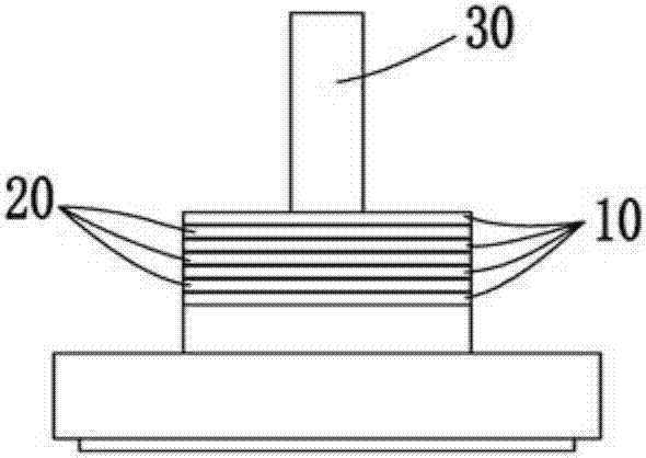
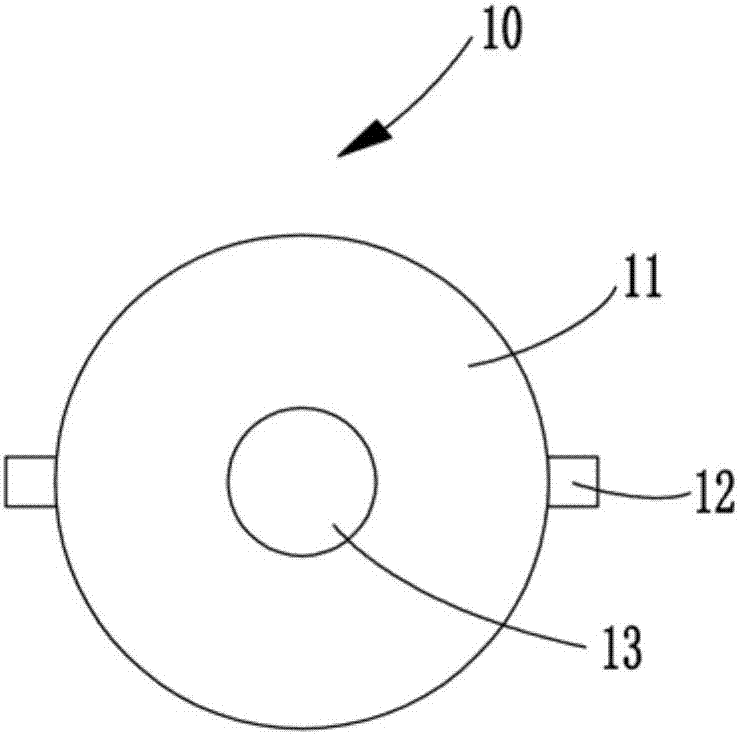
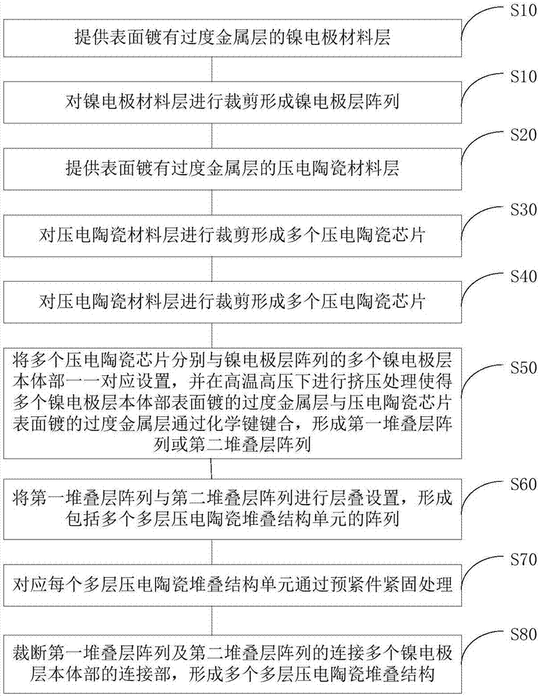
[0015] Embodiments of the present invention will be further described in detail below in conjunction with the accompanying drawings and examples. The detailed description and drawings of the following embodiments are used to illustrate the principle of the present invention, but not to limit the scope of the present invention, that is, the present invention is not limited to the described embodiments.

[0016] In the description of the present invention, it should be noted that unless otherwise specified, the meaning of "several" is one or more; the meaning of "plurality" is two or more; the terms "upper" and "lower" , "Left", "Right", "Inner", "Outer", "Front", "Rear", "Head", "Tail" and other indicated directions or positional relationships are based on the directions shown in the drawings or The positional relationship is only for the convenience of describing the present invention and simplifying the description, but does not indicate or imply that the referred device or e...


PUM


Abstract

The invention relates to a multilayer piezoelectric ceramic stack structure and a preparation method thereof as well as a sensor. The multilayer piezoelectric ceramic stack structure comprises a first stack layer and a second stack layer which are stacked; each of the first stack layer and the second stack layer is a composite stack layer formed by bonding material layers through metallic bonds and comprises a piezoelectric ceramic chip and a nickel electrode layer, wherein a transition metal layer is plated on the surface of the piezoelectric ceramic chip; a transition metal layer is plated on the surface of the nickel electrode layer; the transition metal layer plated on the surface of the piezoelectric ceramic chip and the transition metal layer plated on the surface of the nickel electrode layer are bonded through the metallic bonds; and the first stack layer and the second stack layer which are stacked are firmly connected through a pre-tightening piece. The multilayer piezoelectric ceramic stack structure provided by the invention has the advantages of better frequency response characteristic, smaller stress fluctuation at high temperature and simple structure.

Description

technical field [0001] The invention relates to the technical field of sensors, in particular to a multilayer piezoelectric ceramic stack structure, a sensor and a preparation method thereof. Background technique [0002] The high temperature vibration sensor is mainly to solve the measurement of various vibrations in high temperature environment. In these fields, the sensor works under high temperature conditions, which makes the sensor's amplifying circuit and piezoelectric element easy to fail. [0003] The piezoelectric ceramic stack structure currently used as a piezoelectric element usually has a connection layer and an electrode sheet separately provided between separate piezoelectric ceramic sheets. Although this structure realizes the assembly of piezoelectric elements, due to the existence of the matching gap between the connection layer and the electrode sheet and / or piezoelectric ceramic sheet, when applied in a vibration environment, the above-mentioned piezoel...

Claims


Application Information

Patent Timeline
Patent Type & Authority Applications(China)
IPC IPC(8): H01L41/047H01L41/053H01L41/083H01L41/113H01L41/277H01L41/293G01H11/08
CPCG01H11/08H10N30/872H10N30/877H10N30/886H10N30/503H10N30/302H10N30/057H10N30/063
Inventor 聂泳忠聂川
Owner FATRI UNITED TESTING & CONTROL QUANZHOU TECH CO LTD
Why Eureka
Try Eureka