Check patentability & draft patents in minutes with Patsnap Eureka AI!

Complementary depletion type MOSFET rectifier diode based on NP channels

A rectifier diode, depletion-type technology, applied in the field of diodes, can solve the problems of low power sensitivity, high cut-off voltage, difficult to realize, etc., and achieve the effect of reducing reverse leakage current, low power sensitivity, and high power capacity

Pending Publication Date: 2017-09-22
扬州芯智瑞电子科技有限公司
View PDF2 Cites 1 Cited by
  • Summary
  • Abstract
  • Description
  • Claims
  • Application Information

AI Technical Summary

Problems solved by technology

[0002] In wireless energy transmission applications, Schottky diodes with low turn-on voltage are often used to improve high rectification efficiency at low power input levels; however, due to the limitations of semiconductor processes, it is difficult for Schottky diodes with low turn-on voltage to achieve higher The cut-off voltage of the Schottky diode, which has a strong low power sensitivity, is difficult to achieve high power capacity
In some wireless energy transfer applications that require a wide power dynamic range, Schottky diodes with low turn-on voltage are not suitable
At the same time, the semiconductor process determines that the Schottky diode with low turn-on voltage has a large saturation current, that is, reverse leakage current, which reduces the rectification efficiency of the rectifier

Method used


Image

  • Complementary depletion type MOSFET rectifier diode based on NP channels
  • Complementary depletion type MOSFET rectifier diode based on NP channels
  • Complementary depletion type MOSFET rectifier diode based on NP channels

Examples


Embodiment 1

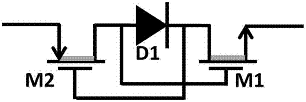
[0016] Such as figure 1 The illustrated rectifier diode based on NP channel complementary depletion-type MOSFETs includes a depletion-type NMOS transistor M1, a depletion-type PMOS transistor M2, and a Schottky diode D1 with a low turn-on voltage. The depletion-type NMOS transistor M1 The drain of the depletion-type PMOS transistor M2 is connected to the cathode of the diode D1, the drain of the depletion-type PMOS transistor M2 is connected to the anode of the diode D1, the gate of the depletion-type NMOS transistor M1 is connected to the anode of the diode D1, and the depletion-type PMOS transistor M2 is connected to the anode of the diode D1. The gate of M2 is connected to the cathode of the diode D1, the source of the depletion-type NMOS transistor M1 is used as the output cathode of the MOSFET rectifier diode, and the source of the depletion-type PMOS transistor is used as the input anode of the MOSFET rectifier diode.

[0017] According to semiconductor knowledge, the dr...

Embodiment 2

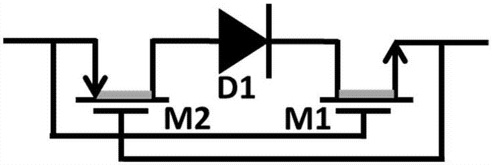
[0035] Such as figure 2 The illustrated rectifier diode based on NP channel complementary depletion-type MOSFETs includes a depletion-type NMOS transistor M1, a depletion-type PMOS transistor M2, and a Schottky diode D1 with a low turn-on voltage. The depletion-type NMOS transistor M1 The drain of the depletion-type NMOS transistor M1 is connected to the cathode of the diode D1, the drain of the depletion-type PMOS transistor M2 is connected to the anode of the diode D1, and the gate of the depletion-type NMOS transistor M1 is connected to the source of the depletion-type PMOS transistor M2. The gate of the depletion-type PMOS transistor M2 is connected to the source of the depletion-type NMOS transistor M1, the source of the depletion-type NMOS transistor M1 is used as the output cathode of the MOSFET rectifier diode, and the source of the depletion-type PMOS transistor is used as the output of the MOSFET rectifier diode Enter positive.

[0036] According to semiconductor k...

Embodiment 3

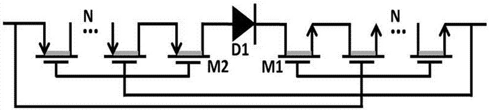
[0053] Such as image 3 A rectifier diode based on NP-channel complementary depletion-type MOSFETs shown, including n depletion-type NMOS transistors M11-M1n, n depletion-type PMOS transistors M21-M2n, and a Schottky diode with low turn-on voltage D1, n depletion-type NMOS transistors M11-M1n are connected in series, that is, the source of M11 is connected to the drain of M12, the source of M12 is connected to the drain of M13, and so on, the source of M1n is used as a MOSFET rectifier The output cathode of the diode, the drain of M11 is connected to the cathode of the diode D1; n depletion-type PMOS transistors M21-M2n are connected in series, that is, the source of M21 is connected to the drain of M22, and the source of M22 is connected to the drain of M23 Connected, and so on, the source of M2n is used as the input anode of the MOSFET rectifier diode, the gates between M11-M1n are connected together and then connected to the source of M2n, and the gates between M21-M2n are ...


PUM


Abstract

The invention discloses a complementary depletion type MOSFET rectifier diode based on NP channels in the field of diodes. The complementary depletion type MOSFET rectifier diode comprises a depletion type NMOS tube M1, a depletion type PMOS tube M2 and a Schottky diode D1 with low turn-on voltage, wherein the drain electrode of the depletion type NMOS tube M1 is connected to the negative side of the diode D1; the drain electrode of the depletion type PMOS tube M2 is connected to the positive side of the diode D1; the grid electrode of the depletion type NMOS tube M1 is connected to the positive side of the diode D1; and the grid electrode of the depletion type PMOS tube M2 is connected to the negative side of the diode D1. The complementary depletion type MOSFET rectifier diode has high performance in the aspects such as low-power sensitivity, high-power capacity and reduction of reverse leakage current, and NP channel depletion type MOS tubes are connected at two ends of the Schottky diode D1 with low turn-on voltage, so that the diode D1 has relatively high cut-off voltage under the premise of low turn-on voltage holding, the effect of protecting the diode D1 from being punctured is achieved preferably, and the complementary depletion type MOSFET rectifier diode can be used for diodes in wireless charging circuits.

Description

technical field [0001] The invention relates to a diode, in particular to a rectifying diode based on the application of wireless energy transmission. Background technique [0002] In wireless energy transmission applications, Schottky diodes with low turn-on voltage are often used to improve high rectification efficiency at low power input levels; however, due to the limitations of semiconductor processes, it is difficult for Schottky diodes with low turn-on voltage to achieve higher The cut-off voltage of the Schottky diode, which has strong low power sensitivity, is difficult to achieve high power capacity. In some wireless energy transfer applications that require a wide power dynamic range, Schottky diodes with low turn-on voltage are not suitable. At the same time, the semiconductor process determines that the Schottky diode with low turn-on voltage has a large saturation current, that is, reverse leakage current, which reduces the rectification efficiency of the rect...

Claims


Application Information

Patent Timeline
IPC IPC(8): H02M7/537
CPCH02M7/537
Inventor 张浩姚鸿
Owner 扬州芯智瑞电子科技有限公司
Features
  • R&D
  • Intellectual Property
  • Life Sciences
  • Materials
  • Tech Scout
  • Unparalleled Data Quality
  • Higher Quality Content
  • 60% Fewer Hallucinations
Learn More