

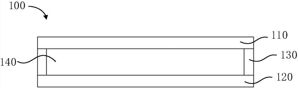
Electro-deposition display component and preparation method thereof
A technology of display components and electrodeposition, applied in nonlinear optics, instruments, optics, etc., can solve problems such as high cost and poor display stability
- Summary
- Abstract
- Description
- Claims
- Application Information
AI Technical Summary
Problems solved by technology
Method used
Image

Examples
preparation example Construction
[0074] see Figure 4 , a method for preparing an electrodeposited display component in one embodiment, comprising the following steps:
[0075] S110, preparing a first electrode film.
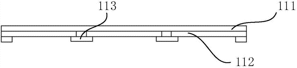
[0076] In one of the embodiments, the step of preparing the first electrode film is as follows: plating a transparent ITO conductive layer on the first substrate, etching the ITO conductive layer so that the electrode pattern appears, and etching the ITO conductive layer Form the first electrode wiring area after etching; plate a transparent first insulating layer on the ITO conductive layer, etch the first insulating layer to expose the electrode pattern of the ITO conductive layer, and make the first insulating layer cover the first electrode wiring area. The prepared first electrode film is used for a partially erasable segment code display component.
[0077] In another embodiment, the step of preparing the first electrode film is as follows: plating a transparent ITO conductive layer on...
Embodiment 1
[0096] (1) Preparation of the first electrode film: Take a glass substrate with a thickness of 0.5 mm, plate it with an ITO conductive film to obtain an ITO glass with a square resistance of 10 ohms, wash with water, wash with acetone, and dry it before use.
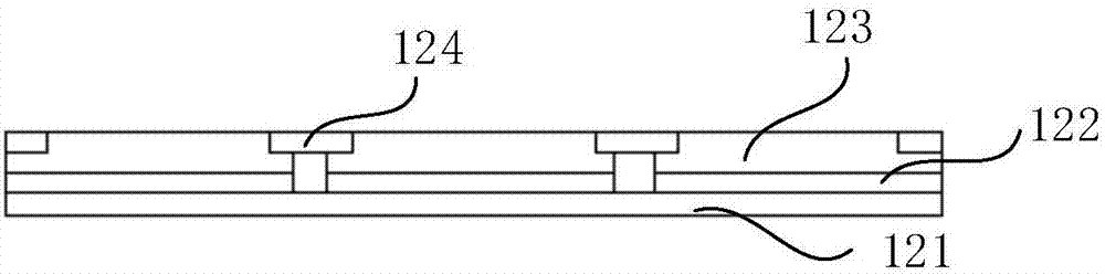
[0097] (2) Preparation of the second electrode film: get a transparent glass with a thickness of 0.5mm slightly larger than the area of the first electrode film, and form a layer of silver conductive layer with a thickness of about 2 μm by magnetron sputtering. Then form a bismuth layer with a thickness of about 5 μm on the silver conductive layer, etch the silver conductive layer and the bismuth layer with 10% nitric acid to make it show electrode patterns; then coat a layer of bismuth with a thickness of about 10 μm. The silicon oxide insulating layer is etched to expose the electrode pattern area; then a bismuth layer is electroplated on the etched area of the silicon dioxide insulating layer until the thickness is...
Embodiment 2
[0105] (1) Preparation of the first electrode film: Take a glass substrate with a thickness of 0.5mm, plate it with an ITO conductive film to obtain an ITO glass with a square resistance of 10 ohms, wash with water, acetone and water, and coat a layer of photoresist , after exposure, etch the electrode pattern with 10% nitric acid, then deposit a silicon dioxide insulating layer with a thickness of 0.2 μm by chemical vapor deposition, and then etch the silicon dioxide insulating layer to display the electrode pattern .
[0106] (2) Preparation of the second electrode film: get a transparent glass with a thickness of 0.5mm slightly larger than the area of the first electrode film, and form a layer of silver conductive layer with a thickness of about 2 μm by magnetron sputtering. Then form a bismuth layer with a thickness of about 10 μm on the silver conductive layer, etch the silver conductive layer and the bismuth layer with 10% nitric acid to make it show electrode patterns...
PUM
| Property | Measurement | Unit |
|---|---|---|
| Thickness | aaaaa | aaaaa |
| Thickness | aaaaa | aaaaa |
| Thickness | aaaaa | aaaaa |
Abstract
Description
Claims
Application Information