Display panel and display device
A display panel and liquid crystal layer technology, applied in nonlinear optics, instruments, optics, etc., can solve the problems of blue sub-pixel area viewing angle deviation, strong blue light intensity, eye damage, etc., to improve viewing angle deviation and reduce blue light Intensity, the effect of reducing the amount of transmission
- Summary
- Abstract
- Description
- Claims
- Application Information
AI Technical Summary
Problems solved by technology
Method used
Image

Examples
no. 1 example
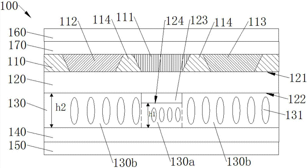
[0040] see figure 2 , the protruding structure 123 and the transparent conductive film layer 125 are made of the same material. The transparent conductive film layer 125 is made of metal oxide, such as indium tin oxide, indium zinc oxide, aluminum tin oxide, aluminum zinc oxide, indium germanium zinc oxide, or other suitable oxides, or is a stack layer of at least two of the above.
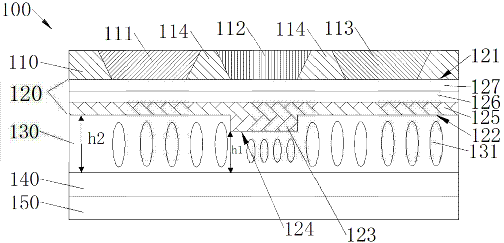
[0041] Optionally, the protruding structure 123 may be formed during the process of preparing the transparent conductive film layer 125 , that is, the patterned transparent conductive film layer 125 is obtained. Under the basic structure of the color filter layer 110, after completing the encapsulation, flattening layer 127 and polarizing layer 126 and other processes, a transparent photoresist structure of unequal height is prepared above the polarizing layer 126. This transparent photoresist structure of unequal height The resistive structure can be completed by photolithography process, and ...
no. 2 example
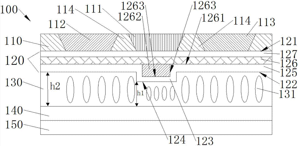
[0043] see image 3 , the polarizing layer 126 has a first top wall 1261 facing the liquid crystal layer 130 . A first protrusion 1262 is disposed on the first top wall 1261 . The first bump 1262 protrudes toward the liquid crystal layer 130 . The first protrusion 1262 has a first peripheral surface 1263 connected to the first top wall 1261 . The functional layer 120 also includes a transparent conductive film layer 125 . The transparent conductive film layer 125 covers the first peripheral surface 1263 to form the protruding structure 123 . That is to say, the protruding structure 123 is formed by the first bump 1262 and the transparent conductive film layer 125 disposed on the first peripheral surface 1263 of the first bump 1262 .
[0044] Optionally, the first bump 1262 and the polarizing layer 126 may be made of the same material or a different material. If the first bumps 1262 and the polarizing layer 126 are made of the same material, the first bumps 1262 can be for...
no. 3 example
[0046] see Figure 4 , the flat layer 127 has a second top wall 1271 facing the liquid crystal layer 130 . A second protrusion 1272 is disposed on the second top wall 1271 , and the second protrusion 1272 protrudes toward the liquid crystal layer 130 . The second protrusion 1272 has a second peripheral surface 1273 connected to the second top wall 1271 . The polarizing layer 126 and the transparent conductive film layer 125 cover the second peripheral surface 1273 to form the protruding structure 123 . Specifically, the polarizing layer 126 covers the second peripheral surface 1273 , and the transparent conductive film layer 125 covers the polarizing layer 126 . That is to say, the protruding structure 123 is formed by the second bump 1272 and the polarizing layer 126 and the transparent conductive film layer 125 disposed on the second peripheral surface 1273 of the second bump 1272 .
[0047] Optionally, the second bump 1272 and the polarizing layer 126 may be made of the ...
PUM
 Abstract
Description
Claims
Application Information
 - R&D
- Intellectual Property
- Life Sciences
- Materials
- Tech Scout
- Unparalleled Data Quality
- Higher Quality Content
- 60% Fewer Hallucinations
Browse by: Latest US Patents, China's latest patents, Technical Efficacy Thesaurus, Application Domain, Technology Topic, Popular Technical Reports.
© 2025 PatSnap. All rights reserved.Legal|Privacy policy|Modern Slavery Act Transparency Statement|Sitemap|About US| Contact US: help@patsnap.com