

Multi-layer circuit structure
A multi-layer circuit and transmission line technology, applied in the directions of printed circuits, printed circuits, printed circuit components, etc., can solve the problems of increased signal transmission loss and reduced signal transmission quality, and can reduce high-frequency signal reflection and impedance discontinuity. point, the effect of improving signal integrity
- Summary
- Abstract
- Description
- Claims
- Application Information
AI Technical Summary
Problems solved by technology
Method used
Image

Examples
Embodiment Construction
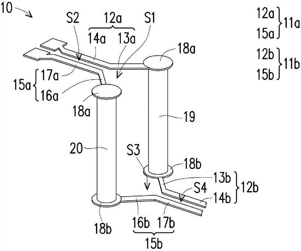
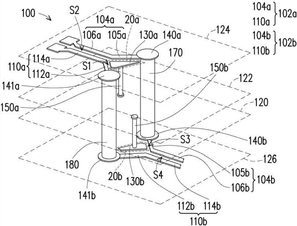
[0052] image 3 is a partial schematic view of a multilayer circuit structure according to an embodiment of the present invention. It should be noted that, for the sake of brevity, image 3 Only the local and differential transmission lines and the reference plane are simply drawn, and the dielectric layer or other lines between the lines of different planes are omitted. see image 3 , the multilayer circuit structure 100 of this embodiment includes two sets of differential transmission line pairs 102a, 102b, two first differential pads 140a, 140b, two second differential pads 141a, 141b, two via holes 170, 180, two sets of conductive patterns 130a, 130b, two blind holes 150a, 150b.
[0053] More specifically, one of the differential transmission line pairs 102a, one of the first differential pads 140a, one of the second differential pads 141a, and one of the groups of conductive patterns 130a are located in one of the circuit layers (such as image 3In the upper plane 124...
PUM
 Abstract
Description
Claims
Application Information